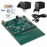
EVAL-ADUC832QSZ Analog Devices Inc, EVAL-ADUC832QSZ Datasheet - Page 39

EVAL-ADUC832QSZ
Manufacturer Part Number
EVAL-ADUC832QSZ
Description
KIT DEV FOR ADUC832 QUICK START
Manufacturer
Analog Devices Inc
Series
QuickStart™ Kitr
Type
MCUr
Specifications of EVAL-ADUC832QSZ
Contents
Evaluation Board, Cable, Power Supply, Software and Documentation
Lead Free Status / RoHS Status
Lead free / RoHS Compliant
For Use With/related Products
ADuC832
Lead Free Status / RoHS Status
Compliant, Lead free / RoHS Compliant
Other names
EVAL-ADUC832QS
EVAL-ADUC832QS
EVAL-ADUC832QS
DRIVING THE ANALOG-TO-DIGITAL CONVERTER
The ADC incorporates a successive approximation (SAR) architec-
ture involving a charge-sampled input stage. Figure 39 shows
the equivalent circuit of the analog input section. Each ADC
conversion is divided into two distinct phases as defined by the
position of the switches in Figure 39. During the sampling
phase (with SW1 and SW2 in the track position), a charge
proportional to the voltage on the analog input is developed
across the input sampling capacitor. During the conversion
phase (with both switches in the hold position) the capacitor
DAC is adjusted via internal SAR logic until the voltage on
Node A is 0, indicating that the sampled charge on the input
capacitor is balanced out by the charge being output by the
capacitor DAC. The digital value finally contained in the SAR
is then latched out as the result of the ADC conversion. Control
of the SAR, and timing of acquisition and sampling modes, is
handled automatically by built-in ADC control logic. Acquisi-
tion and conversion times are also fully configurable under user
control.
Note that whenever a new input channel is selected, a residual
charge from the 32 pF sampling capacitor places a transient on
the newly selected input. The signal source must be capable of
recovering from this transient before the sampling switches are
changed to hold mode. Delays can be inserted in software
(between channel selection and conversion request) to account
for input stage settling, but a hardware solution alleviates this
burden from the software design task and ultimately results in a
cleaner system implementation. One hardware solution would
be to choose a very fast settling op amp to drive each analog
input. Such an op amp would need to fully settle from a small
signal transient in less than 300 ns to guarantee adequate
settling under all software configurations. A better solution,
recommended for use with any amplifier, is shown in Figure 40.
AGND
ADC7
ADC0
TRACK
200Ω
HOLD
200Ω
AGND
DAC1
DAC0
TEMPERATURE SENSOR
V
Figure 39. Internal ADC Structure
REF
TRACK
SW1
NODE A
32pF
ADuC832
HOLD
SW2
COMPARATOR
CAPACITOR
DAC
Rev. A | Page 39 of 92
Though the circuit in Figure 40 may look like a simple
antialiasing filter, it actually serves no such purpose because its
corner frequency is well above the Nyquist frequency, even at a
200 kHz sample rate. Though the R/C does help to reject some
incoming high frequency noise, its primary function is to ensure
that the transient demands of the ADC input stage are met.
It does so by providing a capacitive bank from which the 32 pF
sampling capacitor can draw its charge. Its voltage does not
change by more than one count (1/4096) of the 12-bit transfer
function when the 32 pF charge from a previous channel is
dumped onto it. A larger capacitor can be used if desired, but
not a larger resistor, for the following reasons.
The Schottky diodes in Figure 40 may be necessary to limit
the voltage applied to the analog input pin as per the absolute
maximum ratings (see Table 12). They are not necessary if the
op amp is powered from the same supply as the ADuC832
because in that case the op amp is unable to generate voltages
above V
sary unless the signal source is very low impedance to begin
with. DC leakage currents at the ADuC832 analog inputs can
cause measurable dc errors with external source impedances as
little as ~100 Ω. To ensure accurate ADC operation, keep the
total source impedance at each analog input less than 61 Ω.
Table 19 illustrates examples of how source impedance can
affect dc accuracy.
Table 19. Source Impedance Examples
Source
Impedance
61 Ω
610 Ω
Although Figure 40 shows the op amp operating at a gain of 1, it
can be configured for any gain needed. Also, an instrumentation
amplifier can be easily used in its place to condition differential
signals. Use any modern amplifier that is capable of delivering
the signal (0 V to V
supply rail-to-rail op amps that are useful for this purpose
include, but are not limited to, the ones given in Table 20. Visit
www.analog.com
instrumentation amps.
DD
or below ground. An op amp of some kind is neces-
Figure 40. Buffering Analog Inputs
for details on these and other op amps and
Error from 1 μA
Leakage Current
61 μV = 0.1 LSB
610 μV = 1 LSB
REF
) with minimal saturation. Some single-
10Ω
0.1µF
ADC0
Error from 10 μA
Leakage Current
610 μV = 1 LSB
6.1 mV = 10 LSB
ADuC832
ADuC832


