EVAL-ADUC832QSZ Analog Devices Inc, EVAL-ADUC832QSZ Datasheet - Page 71
EVAL-ADUC832QSZ
Manufacturer Part Number
EVAL-ADUC832QSZ
Description
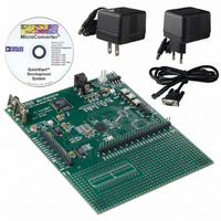
KIT DEV FOR ADUC832 QUICK START
Manufacturer
Analog Devices Inc
Series
QuickStart™ Kitr
Type
MCUr
Specifications of EVAL-ADUC832QSZ
Contents
Evaluation Board, Cable, Power Supply, Software and Documentation
Lead Free Status / RoHS Status
Lead free / RoHS Compliant
For Use With/related Products
ADuC832
Lead Free Status / RoHS Status
Compliant, Lead free / RoHS Compliant
Other names
EVAL-ADUC832QS
EVAL-ADUC832QS
EVAL-ADUC832QS


TCON (Timer/Counter 0 and Timer/Counter 1 Control
Register)
SFR Address:
Power-On Default Value:
Bit Addressable:
Table 37. TCON SFR Bit Designations
Bit
[7]
[6]
[5]
[4]
[3]
[2]
[1]
[0]
1
These bits are not used in the control of Timer/Counter 0 and Timer/Counter 1, but are used instead in the control and monitoring of the external INT0 and INT1
interrupt pins.
Name
TF1
TR1
TF0
TR0
IE1
IT1
IE0
IT0
1
1
1
1
Description
Timer 1 overflow flag.
Set by hardware on a Timer/Counter 1 overflow.
Cleared by hardware when the program counter (PC) vectors to the interrupt service routine.
Timer 1 run control bit.
Set by the user to turn on Timer/Counter 1.
Cleared by the user to turn off Timer/Counter 1.
Timer 0 overflow flag.
Set by hardware on a Timer/Counter 0 overflow.
Cleared by hardware when the PC vectors to the interrupt service routine.
Timer 0 run control bit.
Set by the user to turn on Timer/Counter 0.
Cleared by the user to turn off Timer/Counter 0.
External Interrupt 1 (INT1) flag.
Set by hardware by a falling edge or zero level being applied to external interrupt Pin INT1, depending on the state of Bit IT1.
Cleared by hardware when the PC vectors to the interrupt service routine only if the interrupt was transition-activated. If
level-activated, the external requesting source controls the request flag, rather than the on-chip hardware.
External Interrupt 1 (IE1) trigger type.
Set by software to specify edge-sensitive detection (that is, a 1-to-0 transition).
Cleared by software to specify level-sensitive detection (that is, zero level).
External Interrupt 0 (INT0) flag.
Set by hardware by a falling edge or zero level being applied to external interrupt Pin INT0, depending on the state of Bit IT0.
Cleared by hardware when the PC vectors to the interrupt service routine only if the interrupt was transition-activated.
If level-activated, the external requesting source controls the request flag, rather than the on-chip hardware.
External Interrupt 0 (IE0) trigger type.
Set by software to specify edge-sensitive detection (that is, 1-to-0 transition).
Cleared by software to specify level-sensitive detection (that is, zero level).
88H
00H
Yes
Rev. A | Page 71 of 92
TIMER/COUNTER 0 AND TIMER/COUNTER 1 DATA
REGISTERS
Each timer consists of two 8-bit registers. These can be used as
independent registers or combined to be a single 16-bit register,
depending on the timer mode configuration.
TH0 and TL0
TH0 is the Timer 0 high byte and TL0 is the low byte. The SFR
addresses for TH0 and TL0 are 8CH and 8AH, respectively.
TH1 and TL1
TH1 is the Timer 1 high byte and TH0 is the low byte. The SFR
addresses for TH1 and TL1 are 8DH and 8BH, respectively.
ADuC832
Related parts for EVAL-ADUC832QSZ
Image
Part Number
Description
Manufacturer
Datasheet
Request
R


Part Number:
Description:
BOARD EVAL FOR SI270X-A
Manufacturer:
Silicon Laboratories Inc
Datasheet:

Part Number:
Description:
BUCK CONV REF DESIGN KIT IP1201
Manufacturer:
International Rectifier
Datasheet:
Part Number:
Description:
BOARD DEMO SYNC DUAL BUCK CNVTER
Manufacturer:
International Rectifier
Datasheet:
Part Number:
Description:
BOARD DEMO SYNC BUCK CONVETER
Manufacturer:
International Rectifier
Datasheet:

Part Number:
Description:
EVALBOARD/EB Omnidirectional microphone - Analog
Manufacturer:
Analog Devices
Datasheet:
Part Number:
Description:
EVALBOARD/EB Omnidirectional microphone - Analog
Manufacturer:
Analog Devices
Datasheet:


Part Number:
Description:
BOARD EVAL LED DRIVER LT3756
Manufacturer:
Linear Technology
Datasheet:

Part Number:
Description:
BOARD EVAL FOR AD7741/7742
Manufacturer:
Analog Devices Inc
Datasheet:

Part Number:
Description:
±1.7g Dual-Axis IMEMS Accelerometer Evaluation Board
Manufacturer:
Analog Devices Inc
Datasheet:

Part Number:
Description:
IC MULTIPLIER ANALOG 8-SOIC T/R
Manufacturer:
Analog Devices Inc
Datasheet:

Part Number:
Description:
IC ANALOG MULTIPLIER 8-DIP
Manufacturer:
Analog Devices Inc
Datasheet:
Part Number:
Description:
IC ANALOG MULTIPLIER 8-SOIC
Manufacturer:
Analog Devices Inc
Datasheet:
Part Number:
Description:
IC ANALOG MULTIPLIER 8-DIP
Manufacturer:
Analog Devices Inc
Datasheet: