EVAL-ADUC832QSZ Analog Devices Inc, EVAL-ADUC832QSZ Datasheet - Page 23
EVAL-ADUC832QSZ
Manufacturer Part Number
EVAL-ADUC832QSZ
Description
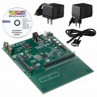
KIT DEV FOR ADUC832 QUICK START
Manufacturer
Analog Devices Inc
Series
QuickStart™ Kitr
Type
MCUr
Specifications of EVAL-ADUC832QSZ
Contents
Evaluation Board, Cable, Power Supply, Software and Documentation
Lead Free Status / RoHS Status
Lead free / RoHS Compliant
For Use With/related Products
ADuC832
Lead Free Status / RoHS Status
Compliant, Lead free / RoHS Compliant
Other names
EVAL-ADUC832QS
EVAL-ADUC832QS
EVAL-ADUC832QS


Mnemonic
P3.4/T0/PWMC/PWM0/EXTCLK
P3.5/T1/CONVST
P3.6/WR
P3.7/RD
SCLOCK
SDATA/MOSI
P2.0/A8/A16
P2.1/A9/A17
P2.2/A10/A18
P2.3/A11/A19
XTAL1
MQFP
22
23
24
25
26
27
28
29
30
31
32
Pin No.
LFCSP
24
25
26
27
28
29
30
31
32
33
34
I
Type
I/O
I
I
O
I
I/O
I
I
I/O
O
O
O
I/O
I/O
I/O
I/O
I/O
I/O
I/O
I/O
I/O
I/O
I/O
Description
Input/Output Port 3 (P3.4). Port 3 is a bidirectional port with internal pull-up resistors.
Port 3 pins that have 1s written to them are pulled high by the internal pull-up
resistors, and in that state can be used as inputs. As inputs, Port 3 pins being pulled
externally low sources current because of the internal pull-up resistors.
Timer/Counter 0 Input (T0).
PWM Clock Input (PWMC).
PWM0 Voltage Output (PWM0). PWM outputs can be configured to uses
Port 2.6 and Port 2.7, or Port 3.4 and Port 3.3.
Input for External Clock Signal (EXTCLK). This pin must be enabled via the CFG832
register.
Input/Output Port 3 (P3.5). Port 3 is a bidirectional port with internal pull-up resistors.
Port 3 pins that have 1s written to them are pulled high by the internal pull-up
resistors, and in that state can be used as inputs. As inputs, Port 3 pins being pulled
externally low sources current because of the internal pull-up resistors.
Timer/Counter 1 Input (T1).
Active Low Convert Start Logic Input for the ADC Block When the External Convert
Start Function is Enabled (CONVST). A low-to-high transition on this input puts the
track-and-hold into its hold mode and starts conversion.
Input/Output Port 3 (P3.6). Port 3 is a bidirectional port with internal pull-up resistors.
Port 3 pins that have 1s written to them are pulled high by the internal pull-up
resistors, and in that state can be used as inputs. As inputs, Port 3 pins being pulled
externally low sources current because of the internal pull-up resistors.
Write Control Signal, Logic Output (WR). Latches the data byte from Port 0 into the
external data memory.
Input/Output Port 3 (P3.7). Port 3 is a bidirectional port with internal pull-up resistors.
Port 3 pins that have 1s written to them are pulled high by the internal pull-up
resistors, and in that state can be used as inputs. As inputs, Port 3 pins being pulled
externally low sources current because of the internal pull-up resistors.
Read Control Signal, Logic Output (RD). Enables the external data memory to Port 0.
Serial Clock Pin for I
User Selectable, I
SPI Master Output/Slave Input Data I/O Pin for SPI Interface (MOSI).
Input/Output Port 2 (P2.0). Port 2 is a bidirectional port with internal pull-up resistors.
Port 2 pins that have 1s written to them are pulled high by the internal pull-up
resistors, and in that state can be used as inputs. As inputs, Port 2 pins being pulled
externally low sources current because of the internal pull-up resistors.
External Memory Addresses (A8/A16). Port 2 emits the high order address bytes
during fetches from external program memory and middle and high order address
bytes during accesses to the external 24-bit external data memory space.
Input/Output Port 2 (P2.1). Port 2 is a bidirectional port with internal pull-up resistors.
Port 2 pins that have 1s written to them are pulled high by the internal pull-up
resistors, and in that state can be used as inputs. As inputs, Port 2 pins being pulled
externally low sources current because of the internal pull-up resistors.
External Memory Addresses (A9/A17). Port 2 emits the high order address bytes
during fetches from external program memory and middle and high order address
bytes during accesses to the external 24-bit external data memory space.
Input/Output Port 2 (P2.2). Port 2 is a bidirectional port with internal pull-up resistors.
Port 2 pins that have 1s written to them are pulled high by the internal pull-up
resistors, and in that state can be used as inputs. As inputs, Port 2 pins being pulled
externally low sources current because of the internal pull-up resistors.
External Memory Addresses (A10/A18). Port 2 emits the high order address bytes
during fetches from external program memory and middle and high order address
bytes during accesses to the external 24-bit external data memory space.
Input/Output Port 2 (P2.3). Port 2 is a bidirectional port with internal pull-up resistors.
Port 2 pins that have 1s written to them are pulled high by the internal pull-up
resistors, and in that state can be used as inputs. As inputs, Port 2 pins being pulled
externally low sources current because of the internal pull-up resistors.
External Memory Addresses (A11/A19). Port 2 emits the high order address bytes
during fetches from external program memory and middle and high order address
bytes during accesses to the external 24-bit external data memory space.
Input to the Inverting Oscillator Amplifier.
Rev. A | Page 23 of 92
2
C-Compatible or SPI Data Input/Output Pin (SDATA).
2
C-Compatible or SPI Serial Interface Clock.
ADuC832
Related parts for EVAL-ADUC832QSZ
Image
Part Number
Description
Manufacturer
Datasheet
Request
R


Part Number:
Description:
BOARD EVAL FOR SI270X-A
Manufacturer:
Silicon Laboratories Inc
Datasheet:

Part Number:
Description:
BUCK CONV REF DESIGN KIT IP1201
Manufacturer:
International Rectifier
Datasheet:
Part Number:
Description:
BOARD DEMO SYNC DUAL BUCK CNVTER
Manufacturer:
International Rectifier
Datasheet:
Part Number:
Description:
BOARD DEMO SYNC BUCK CONVETER
Manufacturer:
International Rectifier
Datasheet:

Part Number:
Description:
EVALBOARD/EB Omnidirectional microphone - Analog
Manufacturer:
Analog Devices
Datasheet:
Part Number:
Description:
EVALBOARD/EB Omnidirectional microphone - Analog
Manufacturer:
Analog Devices
Datasheet:


Part Number:
Description:
BOARD EVAL LED DRIVER LT3756
Manufacturer:
Linear Technology
Datasheet:

Part Number:
Description:
BOARD EVAL FOR AD7741/7742
Manufacturer:
Analog Devices Inc
Datasheet:

Part Number:
Description:
±1.7g Dual-Axis IMEMS Accelerometer Evaluation Board
Manufacturer:
Analog Devices Inc
Datasheet:

Part Number:
Description:
IC MULTIPLIER ANALOG 8-SOIC T/R
Manufacturer:
Analog Devices Inc
Datasheet:

Part Number:
Description:
IC ANALOG MULTIPLIER 8-DIP
Manufacturer:
Analog Devices Inc
Datasheet:
Part Number:
Description:
IC ANALOG MULTIPLIER 8-SOIC
Manufacturer:
Analog Devices Inc
Datasheet:
Part Number:
Description:
IC ANALOG MULTIPLIER 8-DIP
Manufacturer:
Analog Devices Inc
Datasheet: