AD9958/PCB Analog Devices Inc, AD9958/PCB Datasheet - Page 24
AD9958/PCB
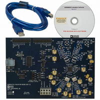
Manufacturer Part Number
AD9958/PCB
Description
BOARD EVALUATION FOR AD9958
Manufacturer
Analog Devices Inc
Datasheet
1.AD9958BCPZ.pdf
(44 pages)
Specifications of AD9958/PCB
Design Resources
Low Jitter Sampling Clock Generator for High Performance ADCs Using AD9958/9858 and AD9515 (CN0109) Phase Coherent FSK Modulator (CN0186)
Lead Free Status / RoHS Status
Contains lead / RoHS non-compliant
Available stocks
Company
Part Number
Manufacturer
Quantity
Price
Company:

Part Number:
AD9958/PCBZ
Manufacturer:
Analog Devices Inc
Quantity:
135


AD9958
MODULATION USING SDIO_x PINS FOR RU/RD
For RU/RD bits = 11, the SDIO_1, SDIO_2, and SDIO_3 pins
are available for RU/RD. In this mode, modulation levels of 2, 4,
and 16 are available. Note that the serial I/O port can be used only
in 1-bit serial mode.
Two-Level Modulation Using SDIO Pins for RU/RD
Table 15. Profile Pin and Channel Assignments in Two-Level
Modulation (RU/RD Enabled)
Profile Pin Config. (PPC)
(FR1[14:12])
XXX
For the configuration in Table 15, each profile pin is dedicated
to a specific channel. In this case, the SDIO_x pins can be used
for the RU/RD function, as described in Table 16.
Four-Level Modulation Using SDIO Pins for RU/RD
For RU/RD bits = 11 (the SDIO_1 and SDIO_2 pins are avail-
able for RU/RD), the modulation level is set to 4. See Table 17
for pin assignments, including SDIO_x pin assignments.
Table 16. Channel and SDIO_1/SDIO_2/SDIO_3 Pin Assignments for RU/RD Operation
SDIO_1
1
1
1
1
Table 17. Channel and Profile Pin Assignments, Including SDIO_1/SDIO_2/SDIO_3 Pin Assignments for RU/RD Operation
Profile Pin Configuration (PPC) (FR1[14:12])
101
Table 18. Channel and Profile Pin Assignments, Including SDIO_1 Pin Assignments for RU/RD Operation
Profile Pin Configuration (PPC) (FR1[14:12])
X10
X11
SDIO_2
0
0
1
1
P0
N/A
SDIO_3
0
1
0
1
P1
N/A
P2
CH0
Description
Triggers the ramp-up function for CH0
Triggers the ramp-down function for CH0
Triggers the ramp-up function for CH1
Triggers the ramp-down function for CH1
P0
CH0
CH1
P0
CH0
P3
CH1
Rev. A | Page 24 of 44
P1
CH0
P1
CH0
CH1
P2
CH1
P2
CH0
CH1
For the configuration shown in Table 17, the profile (channel
word) register is chosen based on the 2-bit value presented to
Profile Pins [P1:P2] or [P3:P4].
For example, if PPC = 101, [P0:P1] = 11, and [P2:P3] = 01, the
contents of the Channel Word 3 register of Channel 0 are
presented to the output of Channel 0 and the contents of the
Channel Word 1 register of Channel 1 are presented to the
output of Channel 1. SDIO_1 and SDIO_2 provide the RU/RD
function.
16-Level Modulation Using SDIO Pins for RU/RD
The RU/RD bits = 11 (SDIO_1 available for RU/RD), and the
level is set to 16. See the pin assignments shown in Table 18.
For the configuration shown in Table 18, the profile (channel
word) register is chosen based on the 4-bit value presented to
Profile Pins [P0:P3]. For example, if PPC = X10 and [P0:P3] =
1101, then the contents of the Channel Word 13 register of
Channel 0 is presented to the output of Channel 0. The SDIO_1
pin provides the RU/RD function.
P3
CH1
P3
CH0
CH1
SDIO_1
CH0 RU/RD
CH1 RU/RD
SDIO_1
CH0 RU/RD
SDIO_2
CH1 RU/RD
SDIO_2
N/A
N/A
N/A
SDIO_3
SDIO_3
N/A
N/A
Related parts for AD9958/PCB
Image
Part Number
Description
Manufacturer
Datasheet
Request
R

Part Number:
Description:
BOARD EVALUATION FOR AD9958
Manufacturer:
Analog Devices Inc
Datasheet:


Part Number:
Description:
±1.7g Dual-Axis IMEMS Accelerometer Evaluation Board
Manufacturer:
Analog Devices Inc
Datasheet:

Part Number:
Description:
Inertial Sensor Evaluation System
Manufacturer:
Analog Devices Inc
Datasheet:
Part Number:
Description:
Manufacturer:
Analog Devices Inc
Datasheet:
Part Number:
Description:
Manufacturer:
Analog Devices Inc
Datasheet:
Part Number:
Description:
Manufacturer:
Analog Devices Inc
Datasheet:
Part Number:
Description:
Manufacturer:
Analog Devices Inc
Datasheet:
Part Number:
Description:
Manufacturer:
Analog Devices Inc
Datasheet:
Part Number:
Description:
Manufacturer:
Analog Devices Inc
Datasheet:
Part Number:
Description:
Manufacturer:
Analog Devices Inc
Datasheet:
Part Number:
Description:
Manufacturer:
Analog Devices Inc
Datasheet:
Part Number:
Description:
Manufacturer:
Analog Devices Inc
Datasheet: