AD9958/PCB Analog Devices Inc, AD9958/PCB Datasheet - Page 9
AD9958/PCB
Manufacturer Part Number
AD9958/PCB
Description
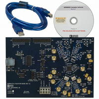
BOARD EVALUATION FOR AD9958
Manufacturer
Analog Devices Inc
Datasheet
1.AD9958BCPZ.pdf
(44 pages)
Specifications of AD9958/PCB
Design Resources
Low Jitter Sampling Clock Generator for High Performance ADCs Using AD9958/9858 and AD9515 (CN0109) Phase Coherent FSK Modulator (CN0186)
Lead Free Status / RoHS Status
Contains lead / RoHS non-compliant
Available stocks
Company
Part Number
Manufacturer
Quantity
Price
Company:

Part Number:
AD9958/PCBZ
Manufacturer:
Analog Devices Inc
Quantity:
135


PIN CONFIGURATION AND FUNCTION DESCRIPTIONS
Table 3. Pin Function Descriptions
Pin No.
1
2
3
4
5, 7, 11, 15, 19, 21,
26, 29, 30, 31, 33,
35, 36, 37, 39
6, 10, 12, 16, 18,
20, 25
45, 55
44, 56
8
9
13
14
17
22
23
Mnemonic
SYNC_IN
SYNC_OUT
MASTER_RESET
PWR_DWN_CTL
AVDD
AGND
DVDD
DGND
CH0_IOUT
CH0_IOUT
CH1_IOUT
CH1_IOUT
DAC_RSET
REF_CLK
REF_CLK
MASTER_RESET
NOTES
1. THE EXPOSED EPAD ON BOTTOM SIDE OF PACKAGE IS AN
2. PIN 49 IS DVDD_I/O AND IS TIED TO 3.3V.
3. NC = NO CONNECT.
PWR_DWN_CTL
ELECTRICAL CONNECTION AND MUST BE SOLDERED TO GROUND.
SYNC_OUT
CH0_IOUT
CH0_IOUT
CH1_IOUT
CH1_IOUT
SYNC_IN
I/O
I
O
I
I
I
I
I
I
O
O
O
O
I
I
I
AGND
AGND
AGND
AVDD
AVDD
AVDD
1
10
11
12
13
14
1
2
3
4
5
6
7
8
9
Description
Used to Synchronize Multiple AD9958 Devices. Connects to the SYNC_OUT pin of
the master AD9958 device.
Used to Synchronize Multiple AD9958 Devices. Connects to the SYNC_IN pin of the
slave AD9958 devices.
Active High Reset Pin. Asserting the MASTER_RESET pin forces the AD9958 internal
registers to their default state, as described in the Register Maps and Bit Descriptions
section.
External Power-Down Control.
Analog Power Supply Pins (1.8 V).
Analog Ground Pins.
Digital Power Supply Pins (1.8 V).
Digital Power Ground Pins.
True DAC Output. Terminates into AVDD.
Complementary DAC Output. Terminates into AVDD.
True DAC Output. Terminates into AVDD.
Complementary DAC Output. Terminates into AVDD.
Establishes the Reference Current for All DACs. A 1.91 kΩ resistor (nominal) is
connected from Pin 17 to AGND.
Complementary Reference Clock/Oscillator Input. When the REF_CLK is operated
in single-ended mode, this pin should be decoupled to AVDD or AGND with a
0.1 μF capacitor.
Reference Clock/Oscillator Input. When the REF_CLK is operated in single-ended
mode, this is the input. See the Modes of Operation section for the reference clock
configuration.
Figure 3. Pin Configuration
PIN 1
INDICATOR
Rev. A | Page 9 of 44
(Not to Scale)
TOP VIEW
AD9958
42
41
40
39
38
37
36
35
34
33
32
31
30
29
P2
P1
P0
AVDD
NC
AVDD
AVDD
AVDD
NC
AVDD
NC
AVDD
AVDD
AVDD
AD9958
Related parts for AD9958/PCB
Image
Part Number
Description
Manufacturer
Datasheet
Request
R

Part Number:
Description:
BOARD EVALUATION FOR AD9958
Manufacturer:
Analog Devices Inc
Datasheet:


Part Number:
Description:
±1.7g Dual-Axis IMEMS Accelerometer Evaluation Board
Manufacturer:
Analog Devices Inc
Datasheet:

Part Number:
Description:
Inertial Sensor Evaluation System
Manufacturer:
Analog Devices Inc
Datasheet:
Part Number:
Description:
Manufacturer:
Analog Devices Inc
Datasheet:
Part Number:
Description:
Manufacturer:
Analog Devices Inc
Datasheet:
Part Number:
Description:
Manufacturer:
Analog Devices Inc
Datasheet:
Part Number:
Description:
Manufacturer:
Analog Devices Inc
Datasheet:
Part Number:
Description:
Manufacturer:
Analog Devices Inc
Datasheet:
Part Number:
Description:
Manufacturer:
Analog Devices Inc
Datasheet:
Part Number:
Description:
Manufacturer:
Analog Devices Inc
Datasheet:
Part Number:
Description:
Manufacturer:
Analog Devices Inc
Datasheet:
Part Number:
Description:
Manufacturer:
Analog Devices Inc
Datasheet: