AD9958/PCB Analog Devices Inc, AD9958/PCB Datasheet - Page 4
AD9958/PCB
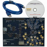
Manufacturer Part Number
AD9958/PCB
Description
BOARD EVALUATION FOR AD9958
Manufacturer
Analog Devices Inc
Datasheet
1.AD9958BCPZ.pdf
(44 pages)
Specifications of AD9958/PCB
Design Resources
Low Jitter Sampling Clock Generator for High Performance ADCs Using AD9958/9858 and AD9515 (CN0109) Phase Coherent FSK Modulator (CN0186)
Lead Free Status / RoHS Status
Contains lead / RoHS non-compliant
Available stocks
Company
Part Number
Manufacturer
Quantity
Price
Company:

Part Number:
AD9958/PCBZ
Manufacturer:
Analog Devices Inc
Quantity:
135


AD9958
SPECIFICATIONS
AVDD and DVDD = 1.8 V ± 5%; DVDD_I/O = 3.3 V ± 5%; T = 25°C; R
(REFCLK multiplier bypassed), unless otherwise noted.
Table 1.
Parameter
REFERENCE CLOCK INPUT CHARACTERISTICS
DAC OUTPUT CHARACTERISTICS
WIDEBAND SFDR
NARROW-BAND SFDR
Resolution
Full-Scale Output Current
Gain Error
Channel-to-Channel Output Amplitude Matching Error
Output Current Offset
Differential Nonlinearity
Integral Nonlinearity
Output Capacitance
Voltage Compliance Range
Channel-to-Channel Isolation
1 MHz to 20 MHz Analog Output
20 MHz to 60 MHz Analog Output
60 MHz to 100 MHz Analog Output
100 MHz to 150 MHz Analog Output
150 MHz to 200 MHz Analog Output
1.1 MHz Analog Output (±10 kHz)
1.1 MHz Analog Output (±50 kHz)
1.1 MHz Analog Output (±250 kHz)
1.1 MHz Analog Output (±1 MHz)
15.1 MHz Analog Output (±10 kHz)
15.1 MHz Analog Output (±50 kHz)
15.1 MHz Analog Output (±250 kHz)
15.1 MHz Analog Output (±1 MHz)
40.1 MHz Analog Output (±10 kHz)
40.1 MHz Analog Output (±50 kHz)
40.1 MHz Analog Output (±250 kHz)
40.1 MHz Analog Output (±1 MHz)
75.1 MHz Analog Output (±10 kHz)
Frequency Range
REFCLK Multiplier Bypassed
REFCLK Multiplier Enabled
Internal VCO Output Frequency Range
Crystal REFCLK Source Range
Input Level
Input Voltage Bias Level
Input Capacitance
Input Impedance
Duty Cycle with REFCLK Multiplier Bypassed
Duty Cycle with REFCLK Multiplier Enabled
CLK Mode Select (Pin 24) Logic 1 Voltage
CLK Mode Select (Pin 24) Logic 0 Voltage
VCO Gain Control Bit Set High
VCO Gain Control Bit Set Low
1
1
Min
1
10
255
100
20
200
45
35
1.25
1.25
−10
−2.5
AVDD −
0.50
72
Rev. A | Page 4 of 44
Typ
1.15
2
1500
±0.5
±1.0
3
−65
−62
−59
−56
−53
−90
−88
−85
−90
−87
−85
−83
−90
−87
−84
−82
−87
1
−86
SET
= 1.91 kΩ; external reference clock frequency = 500 MSPS
Max
500
125
500
160
30
1000
55
65
1.8
0.5
10
10
+10
+2.5
25
AVDD +
0.50
Unit
MHz
mV
Ω
%
%
V
V
% FS
dBc
dBc
dBc
dBc
dBc
dBc
MHz
MHz
MHz
MHz
V
pF
Bits
mA
%
μA
LSB
LSB
pF
V
dB
dBc
dBc
dBc
dBc
dBc
dBc
dBc
dBc
dBc
dBc
dBc
dBc
Test Conditions/Comments
See
Measured at each pin (single-ended)
1.8 V digital input logic
1.8 V digital input logic
Must be referenced to AVDD
DAC supplies tied together (see
The frequency range for wideband SFDR
is defined as dc to Nyquist
Figure 34
and
Figure 35
Figure 19
)
Related parts for AD9958/PCB
Image
Part Number
Description
Manufacturer
Datasheet
Request
R

Part Number:
Description:
BOARD EVALUATION FOR AD9958
Manufacturer:
Analog Devices Inc
Datasheet:


Part Number:
Description:
±1.7g Dual-Axis IMEMS Accelerometer Evaluation Board
Manufacturer:
Analog Devices Inc
Datasheet:

Part Number:
Description:
Inertial Sensor Evaluation System
Manufacturer:
Analog Devices Inc
Datasheet:
Part Number:
Description:
Manufacturer:
Analog Devices Inc
Datasheet:
Part Number:
Description:
Manufacturer:
Analog Devices Inc
Datasheet:
Part Number:
Description:
Manufacturer:
Analog Devices Inc
Datasheet:
Part Number:
Description:
Manufacturer:
Analog Devices Inc
Datasheet:
Part Number:
Description:
Manufacturer:
Analog Devices Inc
Datasheet:
Part Number:
Description:
Manufacturer:
Analog Devices Inc
Datasheet:
Part Number:
Description:
Manufacturer:
Analog Devices Inc
Datasheet:
Part Number:
Description:
Manufacturer:
Analog Devices Inc
Datasheet:
Part Number:
Description:
Manufacturer:
Analog Devices Inc
Datasheet: