AD9958/PCB Analog Devices Inc, AD9958/PCB Datasheet - Page 41
AD9958/PCB
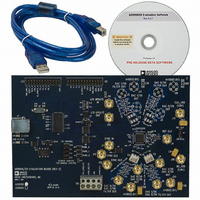
Manufacturer Part Number
AD9958/PCB
Description
BOARD EVALUATION FOR AD9958
Manufacturer
Analog Devices Inc
Datasheet
1.AD9958BCPZ.pdf
(44 pages)
Specifications of AD9958/PCB
Design Resources
Low Jitter Sampling Clock Generator for High Performance ADCs Using AD9958/9858 and AD9515 (CN0109) Phase Coherent FSK Modulator (CN0186)
Lead Free Status / RoHS Status
Contains lead / RoHS non-compliant
Available stocks
Company
Part Number
Manufacturer
Quantity
Price
Company:

Part Number:
AD9958/PCBZ
Manufacturer:
Analog Devices Inc
Quantity:
135


DESCRIPTIONS FOR CHANNEL REGISTERS
Channel Function Register (CFR)—Address 0x03
Three bytes are assigned to this register.
Table 34. Bit Descriptions for CFR
Bit
23:22
21:16
15
14
13
12:11
10
9:8
7
6
5
4
3
2
1
0
Mnemonic
Amplitude frequency
phase (AFP) select
Open
Linear sweep no-dwell
Linear sweep enable
Load SRR at
I/O_UPDATE
Open
Must be 0
DAC full-scale current
control
Digital power-down
DAC power-down
Matched pipe delays
active
Autoclear sweep
accumulator
Clear sweep
accumulator
Autoclear phase
accumulator
Clear phase
accumulator
Sine wave output
enable
Description
Controls what type of modulation is to be performed for that channel. See the Modulation Mode section
for details.
0 = the linear sweep no-dwell function is inactive (default).
1 = the linear sweep no-dwell function is active. If CFR[15] is active, the linear sweep no-dwell function is
activated. See the Linear Sweep Mode section for details. If CFR[14] is clear, this bit is don’t care.
0 = the linear sweep capability is inactive (default).
1 = the linear sweep capability is enabled. When enabled, the delta frequency tuning word is applied to
the frequency accumulator at the programmed ramp rate.
0 = the linear sweep ramp rate timer is loaded only upon timeout (timer = 1) and is not loaded because
of an I/O_UPDATE input signal (default).
1 = the linear sweep ramp rate timer is loaded upon timeout (timer = 1) or at the time of an I/O_UPDATE
input signal.
Must be set to 0.
11 = the DAC is at the largest LSB value (default).
See Table 5 for other settings.
0 = the digital core is enabled for operation (default).
1 = the digital core is disabled and is in its lowest power dissipation state.
0 = the DAC is enabled for operation (default).
1 = the DAC is disabled and is in its lowest power dissipation state.
0 = matched pipe delay mode is inactive (default).
1 = matched pipe delay mode is active. See the Single-Tone Mode—Matched Pipeline Delay section for
details.
0 = the current state of the sweep accumulator is not impacted by receipt of an I/O_UPDATE signal
(default).
1 = the sweep accumulator is automatically and synchronously cleared for one cycle upon receipt of an
I/O_UPDATE signal.
0 = the sweep accumulator functions as normal (default).
1 = the sweep accumulator memory elements are asynchronously cleared.
0 = the current state of the phase accumulator is not impacted by receipt of an I/O_UPDATE signal
(default).
1 = the phase accumulator is automatically and synchronously cleared for one cycle upon receipt of an
I/O_UPDATE signal.
0 = the phase accumulator functions as normal (default).
1 = the phase accumulator memory elements are asynchronously cleared.
0 = the angle-to-amplitude conversion logic employs a cosine function (default).
1 = the angle-to-amplitude conversion logic employs a sine function.
Rev. A | Page 41 of 44
AD9958
Related parts for AD9958/PCB
Image
Part Number
Description
Manufacturer
Datasheet
Request
R

Part Number:
Description:
BOARD EVALUATION FOR AD9958
Manufacturer:
Analog Devices Inc
Datasheet:


Part Number:
Description:
±1.7g Dual-Axis IMEMS Accelerometer Evaluation Board
Manufacturer:
Analog Devices Inc
Datasheet:

Part Number:
Description:
Inertial Sensor Evaluation System
Manufacturer:
Analog Devices Inc
Datasheet:
Part Number:
Description:
Manufacturer:
Analog Devices Inc
Datasheet:
Part Number:
Description:
Manufacturer:
Analog Devices Inc
Datasheet:
Part Number:
Description:
Manufacturer:
Analog Devices Inc
Datasheet:
Part Number:
Description:
Manufacturer:
Analog Devices Inc
Datasheet:
Part Number:
Description:
Manufacturer:
Analog Devices Inc
Datasheet:
Part Number:
Description:
Manufacturer:
Analog Devices Inc
Datasheet:
Part Number:
Description:
Manufacturer:
Analog Devices Inc
Datasheet:
Part Number:
Description:
Manufacturer:
Analog Devices Inc
Datasheet:
Part Number:
Description:
Manufacturer:
Analog Devices Inc
Datasheet: