AD9958/PCB Analog Devices Inc, AD9958/PCB Datasheet - Page 39
AD9958/PCB
Manufacturer Part Number
AD9958/PCB
Description
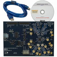
BOARD EVALUATION FOR AD9958
Manufacturer
Analog Devices Inc
Datasheet
1.AD9958BCPZ.pdf
(44 pages)
Specifications of AD9958/PCB
Design Resources
Low Jitter Sampling Clock Generator for High Performance ADCs Using AD9958/9858 and AD9515 (CN0109) Phase Coherent FSK Modulator (CN0186)
Lead Free Status / RoHS Status
Contains lead / RoHS non-compliant
Available stocks
Company
Part Number
Manufacturer
Quantity
Price
Company:

Part Number:
AD9958/PCBZ
Manufacturer:
Analog Devices Inc
Quantity:
135


DESCRIPTIONS FOR CONTROL REGISTERS
Channel Select Register (CSR)—Address 0x00
One byte is assigned to this register.
The CSR determines if channels are enabled or disabled by the status of the two channel enable bits. Both channels are enabled by their
default state. The CSR also determines which serial mode of operation is selected. In addition, the CSR offers a choice of MSB first or LSB
first format.
Table 31. Bit Descriptions for CSR
Bit
7:6
5:4
3
2:1
0
Function Register 1 (FR1)—Address 0x01
Three bytes are assigned to this register. FR1 is used to control the mode of operation of the chip.
Table 32. Bit Descriptions for FR1
Bit
23
22:18
17:16
15
14:12
11:10
9:8
7
Mnemonic
Channel [1:0] enable
Open
Must be 0
Serial I/O mode select
LSB first
Mnemonic
VCO gain control
PLL divider ratio
Charge pump control
Open
Profile pin configuration (PPC)
Ramp-up/ramp-down (RU/RD)
Modulation level
Reference clock input
power-down
Description
Bits are active immediately after being written. They do not require an I/O update to take effect.
There are two sets of channel registers and profile (channel word) registers, one per channel. This
is not shown in the channel register map or the profile register map. The addresses of all channel
registers and profile registers are the same for each channel. Therefore, the channel enable bits
distinguish the channel registers and profile registers values of each channel. For example,
10 = only Channel 1 receives commands from the channel registers and profile registers.
01 = only Channel 0 receives commands from the channel registers and profile registers.
11 = both Channel 0 and Channel 1 receive commands from the channel registers and profile
registers.
Must be set to 0.
00 = single-bit serial (2-wire mode).
01 = single-bit serial (3-wire mode).
10 = 2-bit serial mode.
11 = 4-bit serial mode.
See the Serial I/O Modes of Operation section for more details.
0 = the serial interface accepts serial data in MSB first format (default).
1 = the serial interface accepts serial data in LSB first format.
Description
0 = the low range (system clock below 160 MHz) (default).
1 = the high range (system clock above 255 MHz).
If the value is 4 or 20 (decimal) or between 4 and 20, the PLL is enabled and the value sets the
multiplication factor. If the value is outside of 4 and 20 (decimal), the PLL is disabled.
00 (default) = the charge pump current is 75 μA.
01 = charge pump current is 100 μA.
10 = charge pump current is 125 μA.
11 = charge pump current is 150 μA.
The profile pin configuration bits control the configuration of the data and SDIO_x pins for the
different modulation modes. See the Modulation Mode section in this document for details.
The RU/RD bits control the amplitude ramp-up/ramp-down time of a channel. See the Output
Amplitude Control Mode section for more details.
The modulation (FSK, PSK, and ASK) level bits control the level (2/4/8/16) of modulation to be
performed for a channel. See the Modulation Mode section for more details.
0 = the clock input circuitry is enabled for operation (default).
1 = the clock input circuitry is disabled and is in a low power dissipation state.
Rev. A | Page 39 of 44
AD9958
Related parts for AD9958/PCB
Image
Part Number
Description
Manufacturer
Datasheet
Request
R

Part Number:
Description:
BOARD EVALUATION FOR AD9958
Manufacturer:
Analog Devices Inc
Datasheet:


Part Number:
Description:
±1.7g Dual-Axis IMEMS Accelerometer Evaluation Board
Manufacturer:
Analog Devices Inc
Datasheet:

Part Number:
Description:
Inertial Sensor Evaluation System
Manufacturer:
Analog Devices Inc
Datasheet:
Part Number:
Description:
Manufacturer:
Analog Devices Inc
Datasheet:
Part Number:
Description:
Manufacturer:
Analog Devices Inc
Datasheet:
Part Number:
Description:
Manufacturer:
Analog Devices Inc
Datasheet:
Part Number:
Description:
Manufacturer:
Analog Devices Inc
Datasheet:
Part Number:
Description:
Manufacturer:
Analog Devices Inc
Datasheet:
Part Number:
Description:
Manufacturer:
Analog Devices Inc
Datasheet:
Part Number:
Description:
Manufacturer:
Analog Devices Inc
Datasheet:
Part Number:
Description:
Manufacturer:
Analog Devices Inc
Datasheet:
Part Number:
Description:
Manufacturer:
Analog Devices Inc
Datasheet: