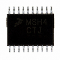
MC9S08SH4CTJ Freescale Semiconductor, MC9S08SH4CTJ Datasheet - Page 159

MC9S08SH4CTJ
Manufacturer Part Number
MC9S08SH4CTJ
Description
IC MCU 8BIT 4K FLASH 20-TSSOP
Manufacturer
Freescale Semiconductor
Series
HCS08r
Datasheet
1.MC9S08SH4CTJ.pdf
(338 pages)
Specifications of MC9S08SH4CTJ
Core Processor
HCS08
Core Size
8-Bit
Speed
40MHz
Connectivity
I²C, LIN, SCI, SPI
Peripherals
LVD, POR, PWM, WDT
Number Of I /o
17
Program Memory Size
4KB (4K x 8)
Program Memory Type
FLASH
Ram Size
256 x 8
Voltage - Supply (vcc/vdd)
2.7 V ~ 5.5 V
Data Converters
A/D 12x10b
Oscillator Type
Internal
Operating Temperature
-40°C ~ 85°C
Package / Case
20-TSSOP
Processor Series
S08SH
Core
HCS08
Data Bus Width
8 bit
Data Ram Size
256 B
Interface Type
SCI/SPI
Maximum Clock Frequency
40 MHz
Number Of Programmable I/os
17
Number Of Timers
3
Operating Supply Voltage
2.7 V to 5.5 V
Maximum Operating Temperature
+ 85 C
Mounting Style
SMD/SMT
3rd Party Development Tools
EWS08
Development Tools By Supplier
DEMO9S08SG32, DEMO9S08SG32AUTO, DEMO9S08SG8, DEMO9S08SG8AUTO, DEMO9S08SH32, DEMO9S08SH8
Minimum Operating Temperature
- 40 C
On-chip Adc
12-ch x 10-bit
A/d Bit Size
10 bit
A/d Channels Available
12
Height
1.05 mm
Length
6.6 mm
Supply Voltage (max)
5.5 V
Supply Voltage (min)
2.7 V
Width
4.5 mm
Lead Free Status / RoHS Status
Lead free / RoHS Compliant
Eeprom Size
-
Lead Free Status / Rohs Status
Lead free / RoHS Compliant
Available stocks
Company
Part Number
Manufacturer
Quantity
Price
Part Number:
MC9S08SH4CTJR
Manufacturer:
FREESCALE
Quantity:
20 000
- Current page: 159 of 338
- Download datasheet (4Mb)
10.4.1.5
The FLL bypassed external (FBE) mode is entered when all the following conditions occur:
In FLL bypassed external mode, the ICSOUT clock is derived from the external reference clock. The FLL
clock is controlled by the external reference clock, and the FLL loop will lock the FLL frequency to 1024
times the reference frequency, as selected by the RDIV bits, so that the ICSLCLK will be available for
BDC communications, and the external reference clock is enabled.
10.4.1.6
The FLL bypassed external low power (FBELP) mode is entered when all the following conditions occur:
In FLL bypassed external low power mode, the ICSOUT clock is derived from the external reference clock
and the FLL is disabled. The ICSLCLK will be not be available for BDC communications. The external
reference clock is enabled.
10.4.1.7
Stop mode is entered whenever the MCU enters a STOP state. In this mode, all ICS clock signals are static
except in the following cases:
ICSIRCLK will be active in stop mode when all the following conditions occur:
ICSERCLK will be active in stop mode when all the following conditions occur:
10.4.2
When switching between FLL engaged internal (FEI) and FLL engaged external (FEE) modes the IREFS
bit can be changed at anytime, but the RDIV bits must be changed simultaneously so that the resulting
frequency stays in the range of 31.25 kHz to 39.0625 kHz. After a change in the IREFS value the FLL will
begin locking again after a few full cycles of the resulting divided reference frequency. The completion of
the switch is shown by the IREFST bit.
Freescale Semiconductor
•
•
•
•
•
•
•
•
•
•
CLKS bits are written to 10.
IREFS bit is written to 0.
BDM mode is active or LP bit is written to 0.
CLKS bits are written to 10.
IREFS bit is written to 0.
BDM mode is not active and LP bit is written to 1.
IRCLKEN bit is written to 1
IREFSTEN bit is written to 1
ERCLKEN bit is written to 1
EREFSTEN bit is written to 1
Mode Switching
FLL Bypassed External (FBE)
FLL Bypassed External Low Power (FBELP)
Stop
MC9S08SH8 MCU Series Data Sheet, Rev. 3
Chapter 10 Internal Clock Source (S08ICSV2)
159
Related parts for MC9S08SH4CTJ
Image
Part Number
Description
Manufacturer
Datasheet
Request
R
Part Number:
Description:
Manufacturer:
Freescale Semiconductor, Inc
Datasheet:
Part Number:
Description:
Manufacturer:
Freescale Semiconductor, Inc
Datasheet:
Part Number:
Description:
Manufacturer:
Freescale Semiconductor, Inc
Datasheet:
Part Number:
Description:
Manufacturer:
Freescale Semiconductor, Inc
Datasheet:
Part Number:
Description:
Manufacturer:
Freescale Semiconductor, Inc
Datasheet:
Part Number:
Description:
Manufacturer:
Freescale Semiconductor, Inc
Datasheet:
Part Number:
Description:
Manufacturer:
Freescale Semiconductor, Inc
Datasheet:
Part Number:
Description:
Manufacturer:
Freescale Semiconductor, Inc
Datasheet:
Part Number:
Description:
Manufacturer:
Freescale Semiconductor, Inc
Datasheet:
Part Number:
Description:
Manufacturer:
Freescale Semiconductor, Inc
Datasheet:
Part Number:
Description:
Manufacturer:
Freescale Semiconductor, Inc
Datasheet:
Part Number:
Description:
Manufacturer:
Freescale Semiconductor, Inc
Datasheet:
Part Number:
Description:
Manufacturer:
Freescale Semiconductor, Inc
Datasheet:
Part Number:
Description:
Manufacturer:
Freescale Semiconductor, Inc
Datasheet:
Part Number:
Description:
Manufacturer:
Freescale Semiconductor, Inc
Datasheet:


