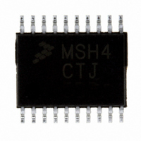
MC9S08SH4CTJ Freescale Semiconductor, MC9S08SH4CTJ Datasheet - Page 77

MC9S08SH4CTJ
Manufacturer Part Number
MC9S08SH4CTJ
Description
IC MCU 8BIT 4K FLASH 20-TSSOP
Manufacturer
Freescale Semiconductor
Series
HCS08r
Datasheet
1.MC9S08SH4CTJ.pdf
(338 pages)
Specifications of MC9S08SH4CTJ
Core Processor
HCS08
Core Size
8-Bit
Speed
40MHz
Connectivity
I²C, LIN, SCI, SPI
Peripherals
LVD, POR, PWM, WDT
Number Of I /o
17
Program Memory Size
4KB (4K x 8)
Program Memory Type
FLASH
Ram Size
256 x 8
Voltage - Supply (vcc/vdd)
2.7 V ~ 5.5 V
Data Converters
A/D 12x10b
Oscillator Type
Internal
Operating Temperature
-40°C ~ 85°C
Package / Case
20-TSSOP
Processor Series
S08SH
Core
HCS08
Data Bus Width
8 bit
Data Ram Size
256 B
Interface Type
SCI/SPI
Maximum Clock Frequency
40 MHz
Number Of Programmable I/os
17
Number Of Timers
3
Operating Supply Voltage
2.7 V to 5.5 V
Maximum Operating Temperature
+ 85 C
Mounting Style
SMD/SMT
3rd Party Development Tools
EWS08
Development Tools By Supplier
DEMO9S08SG32, DEMO9S08SG32AUTO, DEMO9S08SG8, DEMO9S08SG8AUTO, DEMO9S08SH32, DEMO9S08SH8
Minimum Operating Temperature
- 40 C
On-chip Adc
12-ch x 10-bit
A/d Bit Size
10 bit
A/d Channels Available
12
Height
1.05 mm
Length
6.6 mm
Supply Voltage (max)
5.5 V
Supply Voltage (min)
2.7 V
Width
4.5 mm
Lead Free Status / RoHS Status
Lead free / RoHS Compliant
Eeprom Size
-
Lead Free Status / Rohs Status
Lead free / RoHS Compliant
Available stocks
Company
Part Number
Manufacturer
Quantity
Price
Part Number:
MC9S08SH4CTJR
Manufacturer:
FREESCALE
Quantity:
20 000
- Current page: 77 of 338
- Download datasheet (4Mb)
1
2
6.3
The MC9S08SH8 devices contain a feature that allows for up to eight port pins to be tied together
externally to allow higher output current drive. The ganged output drive control register (GNGC) is a
write-once register that is used to enabled the ganged output feature and select which port pins will be used
as ganged outputs. The GNGEN bit in GNGC enables ganged output. The GNGPS[7:1] bits are used to
select which pin will be part of the ganged output.
When GNGEN is set, any pin that is enabled as a ganged output will be automatically configured as an
output and follow the data, drive strength and slew rate control of PTC0. The ganged output drive pin
mapping is shown in
Freescale Semiconductor
Drive Strength
Data Direction
Ganged output not available on 8-pin packages. PTC3-PTC0 not available on 16-pin packages, however PTC0 control
registers are still used to control ganged output.
When GNGEN = 1, PTC0 is forced to an output, regardless of the value in PTCDD0 in PTCDD.
Slew Rate
Port Pin
Control
Control
Control
Control
Data
Ganged Output
2
See the DC characteristics in the electrical section for maximum Port I/O
currents allowed for this MCU.
When a pin is enabled as ganged output, this feature will have priority over
any digital module. An enabled analog function will have priority over the
ganged output pin. See
GNGPS7
PTB5
Table
6-1.
Pin is automatically configured as output when pin is enabled as ganged output.
GNGPS6
PTB4
MC9S08SH8 MCU Series Data Sheet, Rev. 3
Table 6-1. Ganged Output Pin Enable
Table 2-1
PTCDS0 in PTCDS controls drive stength of output
GNGPS5
PTCSE0 in PTCSE controls slew rate of output
PTB3
PTCD0 in PTCD controls data value of output
for information on pin priority. .
NOTE
GNGPS4
GNGC Register Bits
PTB2
GNGPS3
PTC3
GNGPS2
Chapter 6 Parallel Input/Output Control
PTC2
GNGPS1
PTC1
GNGEN
PTC0
1
77
Related parts for MC9S08SH4CTJ
Image
Part Number
Description
Manufacturer
Datasheet
Request
R
Part Number:
Description:
Manufacturer:
Freescale Semiconductor, Inc
Datasheet:
Part Number:
Description:
Manufacturer:
Freescale Semiconductor, Inc
Datasheet:
Part Number:
Description:
Manufacturer:
Freescale Semiconductor, Inc
Datasheet:
Part Number:
Description:
Manufacturer:
Freescale Semiconductor, Inc
Datasheet:
Part Number:
Description:
Manufacturer:
Freescale Semiconductor, Inc
Datasheet:
Part Number:
Description:
Manufacturer:
Freescale Semiconductor, Inc
Datasheet:
Part Number:
Description:
Manufacturer:
Freescale Semiconductor, Inc
Datasheet:
Part Number:
Description:
Manufacturer:
Freescale Semiconductor, Inc
Datasheet:
Part Number:
Description:
Manufacturer:
Freescale Semiconductor, Inc
Datasheet:
Part Number:
Description:
Manufacturer:
Freescale Semiconductor, Inc
Datasheet:
Part Number:
Description:
Manufacturer:
Freescale Semiconductor, Inc
Datasheet:
Part Number:
Description:
Manufacturer:
Freescale Semiconductor, Inc
Datasheet:
Part Number:
Description:
Manufacturer:
Freescale Semiconductor, Inc
Datasheet:
Part Number:
Description:
Manufacturer:
Freescale Semiconductor, Inc
Datasheet:
Part Number:
Description:
Manufacturer:
Freescale Semiconductor, Inc
Datasheet:


