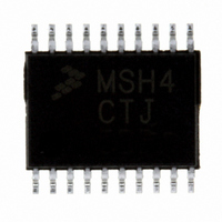
MC9S08SH4CTJ Freescale Semiconductor, MC9S08SH4CTJ Datasheet - Page 29

MC9S08SH4CTJ
Manufacturer Part Number
MC9S08SH4CTJ
Description
IC MCU 8BIT 4K FLASH 20-TSSOP
Manufacturer
Freescale Semiconductor
Series
HCS08r
Datasheet
1.MC9S08SH4CTJ.pdf
(338 pages)
Specifications of MC9S08SH4CTJ
Core Processor
HCS08
Core Size
8-Bit
Speed
40MHz
Connectivity
I²C, LIN, SCI, SPI
Peripherals
LVD, POR, PWM, WDT
Number Of I /o
17
Program Memory Size
4KB (4K x 8)
Program Memory Type
FLASH
Ram Size
256 x 8
Voltage - Supply (vcc/vdd)
2.7 V ~ 5.5 V
Data Converters
A/D 12x10b
Oscillator Type
Internal
Operating Temperature
-40°C ~ 85°C
Package / Case
20-TSSOP
Processor Series
S08SH
Core
HCS08
Data Bus Width
8 bit
Data Ram Size
256 B
Interface Type
SCI/SPI
Maximum Clock Frequency
40 MHz
Number Of Programmable I/os
17
Number Of Timers
3
Operating Supply Voltage
2.7 V to 5.5 V
Maximum Operating Temperature
+ 85 C
Mounting Style
SMD/SMT
3rd Party Development Tools
EWS08
Development Tools By Supplier
DEMO9S08SG32, DEMO9S08SG32AUTO, DEMO9S08SG8, DEMO9S08SG8AUTO, DEMO9S08SH32, DEMO9S08SH8
Minimum Operating Temperature
- 40 C
On-chip Adc
12-ch x 10-bit
A/d Bit Size
10 bit
A/d Channels Available
12
Height
1.05 mm
Length
6.6 mm
Supply Voltage (max)
5.5 V
Supply Voltage (min)
2.7 V
Width
4.5 mm
Lead Free Status / RoHS Status
Lead free / RoHS Compliant
Eeprom Size
-
Lead Free Status / Rohs Status
Lead free / RoHS Compliant
Available stocks
Company
Part Number
Manufacturer
Quantity
Price
Part Number:
MC9S08SH4CTJR
Manufacturer:
FREESCALE
Quantity:
20 000
- Current page: 29 of 338
- Download datasheet (4Mb)
Freescale Semiconductor
1
2
3
4
5
24-pin 20-pin 16-pin
IIC pins can be repositioned using IICPS in SOPT2, default reset locations are on PTA2 and PTA3.
TPM1CHx pins can be repositioned using TPM1PS in SOPT2, default reset locations are on PTA0 and PTB5.
This port pin is part of the ganged output feature. When pin is enabled for ganged output, it will have priority over
all digital modules. The output data, drive strength and slew-rate control of this port pin will follow the configuration
for the PTC0 pin, even in 16-pin packages where PTC0 doesn’t bond out. Ganged output not available in 8-pin
packages.
If ACMP and ADC are both enabled, both will have access to the pin.
Pin is open-drain when configured as output driving high. Pin does not contain a clamp diode to V
not be driven above V
internal gates connected to this pin are pulled to V
10
11
12
13
14
15
16
17
18
19
20
21
22
23
24
1
2
3
4
5
6
7
8
9
Pin Number
10
11
12
13
14
15
16
17
18
19
20
—
—
—
—
3
4
5
6
7
8
9
1
2
—
—
—
—
—
10
11
12
13
14
15
16
—
—
—
3
4
5
6
7
8
9
1
2
DD
. The voltage measured on the internally pulled up RESET will not be pulled to V
Table 2-1. Pin Availability by Package Pin-Count
8-pin
—
—
—
—
—
—
—
—
—
—
—
—
—
—
—
—
3
4
5
6
7
8
1
2
MC9S08SH8 MCU Series Data Sheet, Rev. 3
PTB7
PTB6
PTB5
PTB4
PTC3
PTC2
PTC1
PTC0
PTB3
PTB2
PTB1
PTB0
PTA3
PTA2
PTA1
PTA0
PTA5
PTA4
Port Pin
5
Lowest
SCL
SDA
TPM1CH1
TPM2CH1
PIB3
PIB2
PIB1
PIB0
PIA3
PIA2
PIA1
PIA0
IRQ
ACMPO
DD
Alt 1
1
1
.
2
EXTAL
XTAL
SS
MISO
TPM1CH1
TPM1CH0
MOSI
SPSCK
TxD
RxD
SCL
SDA
TPM2CH0
TPM1CH0
TCLK
Alt 2
1
1
Priority
2
2
2
PTC0
PTC0
PTC0
PTC0
PTC0
PTC0
PTC0
PTC0
Alt 3
3
3
3
3
3
3
3
3
Chapter 2 Pins and Connections
ADP11
ADP10
ADP9
ADP8
ADP7
ADP6
ADP5
ADP4
ADP3
ADP2
ADP1
ADP0
BKGD
Alt 4
Highest
4
4
DD
and should
V
V
ACMP–
ACMP+
MS
DD
SS
RESET
DD
Alt5
. The
4
4
29
Related parts for MC9S08SH4CTJ
Image
Part Number
Description
Manufacturer
Datasheet
Request
R
Part Number:
Description:
Manufacturer:
Freescale Semiconductor, Inc
Datasheet:
Part Number:
Description:
Manufacturer:
Freescale Semiconductor, Inc
Datasheet:
Part Number:
Description:
Manufacturer:
Freescale Semiconductor, Inc
Datasheet:
Part Number:
Description:
Manufacturer:
Freescale Semiconductor, Inc
Datasheet:
Part Number:
Description:
Manufacturer:
Freescale Semiconductor, Inc
Datasheet:
Part Number:
Description:
Manufacturer:
Freescale Semiconductor, Inc
Datasheet:
Part Number:
Description:
Manufacturer:
Freescale Semiconductor, Inc
Datasheet:
Part Number:
Description:
Manufacturer:
Freescale Semiconductor, Inc
Datasheet:
Part Number:
Description:
Manufacturer:
Freescale Semiconductor, Inc
Datasheet:
Part Number:
Description:
Manufacturer:
Freescale Semiconductor, Inc
Datasheet:
Part Number:
Description:
Manufacturer:
Freescale Semiconductor, Inc
Datasheet:
Part Number:
Description:
Manufacturer:
Freescale Semiconductor, Inc
Datasheet:
Part Number:
Description:
Manufacturer:
Freescale Semiconductor, Inc
Datasheet:
Part Number:
Description:
Manufacturer:
Freescale Semiconductor, Inc
Datasheet:
Part Number:
Description:
Manufacturer:
Freescale Semiconductor, Inc
Datasheet:


