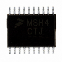
MC9S08SH4CTJ Freescale Semiconductor, MC9S08SH4CTJ Datasheet - Page 91

MC9S08SH4CTJ
Manufacturer Part Number
MC9S08SH4CTJ
Description
IC MCU 8BIT 4K FLASH 20-TSSOP
Manufacturer
Freescale Semiconductor
Series
HCS08r
Datasheet
1.MC9S08SH4CTJ.pdf
(338 pages)
Specifications of MC9S08SH4CTJ
Core Processor
HCS08
Core Size
8-Bit
Speed
40MHz
Connectivity
I²C, LIN, SCI, SPI
Peripherals
LVD, POR, PWM, WDT
Number Of I /o
17
Program Memory Size
4KB (4K x 8)
Program Memory Type
FLASH
Ram Size
256 x 8
Voltage - Supply (vcc/vdd)
2.7 V ~ 5.5 V
Data Converters
A/D 12x10b
Oscillator Type
Internal
Operating Temperature
-40°C ~ 85°C
Package / Case
20-TSSOP
Processor Series
S08SH
Core
HCS08
Data Bus Width
8 bit
Data Ram Size
256 B
Interface Type
SCI/SPI
Maximum Clock Frequency
40 MHz
Number Of Programmable I/os
17
Number Of Timers
3
Operating Supply Voltage
2.7 V to 5.5 V
Maximum Operating Temperature
+ 85 C
Mounting Style
SMD/SMT
3rd Party Development Tools
EWS08
Development Tools By Supplier
DEMO9S08SG32, DEMO9S08SG32AUTO, DEMO9S08SG8, DEMO9S08SG8AUTO, DEMO9S08SH32, DEMO9S08SH8
Minimum Operating Temperature
- 40 C
On-chip Adc
12-ch x 10-bit
A/d Bit Size
10 bit
A/d Channels Available
12
Height
1.05 mm
Length
6.6 mm
Supply Voltage (max)
5.5 V
Supply Voltage (min)
2.7 V
Width
4.5 mm
Lead Free Status / RoHS Status
Lead free / RoHS Compliant
Eeprom Size
-
Lead Free Status / Rohs Status
Lead free / RoHS Compliant
Available stocks
Company
Part Number
Manufacturer
Quantity
Price
Part Number:
MC9S08SH4CTJR
Manufacturer:
FREESCALE
Quantity:
20 000
- Current page: 91 of 338
- Download datasheet (4Mb)
6.6.3.5
6.6.3.6
Freescale Semiconductor
PTCDS[3:0]
GNGP[7:1]
Reset:
Reset:
GNGEN
Field
Field
3:0
7:1
0
W
W
R
R
GNGPS7
Output Drive Strength Selection for Port C Bits — Each of these control bits selects between low and high
output drive for the associated PTC pin. For port C pins that are configured as inputs, these bits have no effect.
0 Low output drive strength selected for port C bit n.
1 High output drive strength selected for port C bit n.
Ganged Output Pin Select Bits— These write-once control bits selects whether the associated pin (see
Table
be controlled by the data, drive strength and slew rate settings for PTCO.
0 Associated pin is not part of the ganged output drive.
1 Assoicated pin is part of the ganged output drive. Requires GNGEN = 1.
Ganged Output Drive Enable Bit— This write-once control bit selects whether the ganged output drive feature
is enabled.
0 Ganged output drive disabled.
1 Ganged output drive enabled. PTC0 forced to output regardless of the value of PTCDD0 in PTCDD.
Port C Drive Strength Selection Register (PTCDS)
0
0
Ganged Output Drive Control Register (GNGC)
0
7
7
6-1for pins available) is enabled for ganged output. When GNGEN = 1, all enabled ganged output pins will
Figure 6-23. Drive Strength Selection for Port C Register (PTCDS)
GNGPS6
Figure 6-24. Ganged Output Drive Control Register (GNGC)
0
0
0
6
6
Table 6-22. PTCDS Register Field Descriptions
Table 6-23. GNGC Register Field Descriptions
MC9S08SH8 MCU Series Data Sheet, Rev. 3
GNGPS5
0
0
0
5
5
GNGPS4
0
0
0
4
4
Description
Description
GNGPS3
PTCDS3
3
0
3
0
GNGPS2
PTCDS2
Chapter 6 Parallel Input/Output Control
0
0
2
2
GNGPS1
PTCDS1
0
0
1
1
PTCDS0
GNGEN
0
0
0
0
91
Related parts for MC9S08SH4CTJ
Image
Part Number
Description
Manufacturer
Datasheet
Request
R
Part Number:
Description:
Manufacturer:
Freescale Semiconductor, Inc
Datasheet:
Part Number:
Description:
Manufacturer:
Freescale Semiconductor, Inc
Datasheet:
Part Number:
Description:
Manufacturer:
Freescale Semiconductor, Inc
Datasheet:
Part Number:
Description:
Manufacturer:
Freescale Semiconductor, Inc
Datasheet:
Part Number:
Description:
Manufacturer:
Freescale Semiconductor, Inc
Datasheet:
Part Number:
Description:
Manufacturer:
Freescale Semiconductor, Inc
Datasheet:
Part Number:
Description:
Manufacturer:
Freescale Semiconductor, Inc
Datasheet:
Part Number:
Description:
Manufacturer:
Freescale Semiconductor, Inc
Datasheet:
Part Number:
Description:
Manufacturer:
Freescale Semiconductor, Inc
Datasheet:
Part Number:
Description:
Manufacturer:
Freescale Semiconductor, Inc
Datasheet:
Part Number:
Description:
Manufacturer:
Freescale Semiconductor, Inc
Datasheet:
Part Number:
Description:
Manufacturer:
Freescale Semiconductor, Inc
Datasheet:
Part Number:
Description:
Manufacturer:
Freescale Semiconductor, Inc
Datasheet:
Part Number:
Description:
Manufacturer:
Freescale Semiconductor, Inc
Datasheet:
Part Number:
Description:
Manufacturer:
Freescale Semiconductor, Inc
Datasheet:


