MC9S08DZ60ACLF Freescale Semiconductor, MC9S08DZ60ACLF Datasheet - Page 278
MC9S08DZ60ACLF
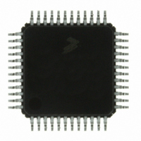
Manufacturer Part Number
MC9S08DZ60ACLF
Description
IC MCU 60K FLASH 4K RAM 48-LQFP
Manufacturer
Freescale Semiconductor
Series
HCS08r
Datasheets
1.DEMO9S08DZ60.pdf
(416 pages)
2.EVB9S08DZ60.pdf
(4 pages)
3.MC9S08DZ48AMLF.pdf
(458 pages)
Specifications of MC9S08DZ60ACLF
Core Processor
HCS08
Core Size
8-Bit
Speed
40MHz
Connectivity
CAN, I²C, LIN, SCI, SPI
Peripherals
LVD, POR, PWM, WDT
Number Of I /o
39
Program Memory Size
60KB (60K x 8)
Program Memory Type
FLASH
Eeprom Size
2K x 8
Ram Size
4K x 8
Voltage - Supply (vcc/vdd)
2.7 V ~ 5.5 V
Data Converters
A/D 16x12b
Oscillator Type
External
Operating Temperature
-40°C ~ 85°C
Package / Case
48-LQFP
Processor Series
S08DZ
Core
HCS08
Data Bus Width
8 bit
Data Ram Size
4 KB
Interface Type
CAN, I2C, SCI, SPI
Maximum Clock Frequency
40 MHz
Number Of Programmable I/os
53
Number Of Timers
2
Operating Supply Voltage
5.5 V
Maximum Operating Temperature
+ 85 C
Mounting Style
SMD/SMT
3rd Party Development Tools
EWS08
Development Tools By Supplier
DEMO9S08DZ60
Minimum Operating Temperature
- 40 C
On-chip Adc
12 bit, 24 Channel
For Use With
DEMO9S08DZ60 - BOARD DEMOEVB9S08DZ60 - BOARD EVAL FOR 9S08DZ60
Lead Free Status / RoHS Status
Lead free / RoHS Compliant
Available stocks
Company
Part Number
Manufacturer
Quantity
Price
Company:

Part Number:
MC9S08DZ60ACLF
Manufacturer:
FREESCAL
Quantity:
1 250
Company:
Part Number:
MC9S08DZ60ACLF
Manufacturer:
Freescale Semiconductor
Quantity:
10 000


Chapter 13 Serial Peripheral Interface (S08SPIV3)
13.2
The SPI optionally shares four port pins. The function of these pins depends on the settings of SPI control
bits. When the SPI is disabled (SPE = 0), these four pins revert to being general-purpose port I/O pins that
are not controlled by the SPI.
13.2.1
When the SPI is enabled as a slave, this pin is the serial clock input. When the SPI is enabled as a master,
this pin is the serial clock output.
13.2.2
When the SPI is enabled as a master and SPI pin control zero (SPC0) is 0 (not bidirectional mode), this
pin is the serial data output. When the SPI is enabled as a slave and SPC0 = 0, this pin is the serial data
input. If SPC0 = 1 to select single-wire bidirectional mode, and master mode is selected, this pin becomes
the bidirectional data I/O pin (MOMI). Also, the bidirectional mode output enable bit determines whether
the pin acts as an input (BIDIROE = 0) or an output (BIDIROE = 1). If SPC0 = 1 and slave mode is
selected, this pin is not used by the SPI and reverts to being a general-purpose port I/O pin.
13.2.3
When the SPI is enabled as a master and SPI pin control zero (SPC0) is 0 (not bidirectional mode), this
pin is the serial data input. When the SPI is enabled as a slave and SPC0 = 0, this pin is the serial data
output. If SPC0 = 1 to select single-wire bidirectional mode, and slave mode is selected, this pin becomes
the bidirectional data I/O pin (SISO) and the bidirectional mode output enable bit determines whether the
pin acts as an input (BIDIROE = 0) or an output (BIDIROE = 1). If SPC0 = 1 and master mode is selected,
this pin is not used by the SPI and reverts to being a general-purpose port I/O pin.
13.2.4
When the SPI is enabled as a slave, this pin is the low-true slave select input. When the SPI is enabled as
a master and mode fault enable is off (MODFEN = 0), this pin is not used by the SPI and reverts to being
a general-purpose port I/O pin. When the SPI is enabled as a master and MODFEN = 1, the slave select
output enable bit determines whether this pin acts as the mode fault input (SSOE = 0) or as the slave select
output (SSOE = 1).
278
External Signal Description
SPSCK — SPI Serial Clock
MOSI — Master Data Out, Slave Data In
MISO — Master Data In, Slave Data Out
SS — Slave Select
BUS CLOCK
SPPR2:SPPR1:SPPR0
1, 2, 3, 4, 5, 6, 7, or 8
Figure 13-4. SPI Baud Rate Generation
MC9S08DZ60 Series Data Sheet, Rev. 4
PRESCALER
DIVIDE BY
2, 4, 8, 16, 32, 64, 128, or 256
CLOCK RATE DIVIDER
SPR2:SPR1:SPR0
DIVIDE BY
Freescale Semiconductor
MASTER
SPI
BIT RATE
Related parts for MC9S08DZ60ACLF
Image
Part Number
Description
Manufacturer
Datasheet
Request
R

Part Number:
Description:
Manufacturer:
Freescale Semiconductor, Inc
Datasheet:
Part Number:
Description:
Manufacturer:
Freescale Semiconductor, Inc
Datasheet:
Part Number:
Description:
Manufacturer:
Freescale Semiconductor, Inc
Datasheet:
Part Number:
Description:
Manufacturer:
Freescale Semiconductor, Inc
Datasheet:
Part Number:
Description:
Manufacturer:
Freescale Semiconductor, Inc
Datasheet:
Part Number:
Description:
Manufacturer:
Freescale Semiconductor, Inc
Datasheet:
Part Number:
Description:
Manufacturer:
Freescale Semiconductor, Inc
Datasheet:
Part Number:
Description:
Manufacturer:
Freescale Semiconductor, Inc
Datasheet:
Part Number:
Description:
Manufacturer:
Freescale Semiconductor, Inc
Datasheet:
Part Number:
Description:
Manufacturer:
Freescale Semiconductor, Inc
Datasheet:
Part Number:
Description:
Manufacturer:
Freescale Semiconductor, Inc
Datasheet:
Part Number:
Description:
Manufacturer:
Freescale Semiconductor, Inc
Datasheet:
Part Number:
Description:
Manufacturer:
Freescale Semiconductor, Inc
Datasheet:
Part Number:
Description:
Manufacturer:
Freescale Semiconductor, Inc
Datasheet:
Part Number:
Description:
Manufacturer:
Freescale Semiconductor, Inc
Datasheet: