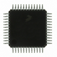
MC9S08DZ60ACLF Freescale Semiconductor, MC9S08DZ60ACLF Datasheet - Page 370

MC9S08DZ60ACLF
Manufacturer Part Number
MC9S08DZ60ACLF
Description
IC MCU 60K FLASH 4K RAM 48-LQFP
Manufacturer
Freescale Semiconductor
Series
HCS08r
Datasheets
1.DEMO9S08DZ60.pdf
(416 pages)
2.EVB9S08DZ60.pdf
(4 pages)
3.MC9S08DZ48AMLF.pdf
(458 pages)
Specifications of MC9S08DZ60ACLF
Core Processor
HCS08
Core Size
8-Bit
Speed
40MHz
Connectivity
CAN, I²C, LIN, SCI, SPI
Peripherals
LVD, POR, PWM, WDT
Number Of I /o
39
Program Memory Size
60KB (60K x 8)
Program Memory Type
FLASH
Eeprom Size
2K x 8
Ram Size
4K x 8
Voltage - Supply (vcc/vdd)
2.7 V ~ 5.5 V
Data Converters
A/D 16x12b
Oscillator Type
External
Operating Temperature
-40°C ~ 85°C
Package / Case
48-LQFP
Processor Series
S08DZ
Core
HCS08
Data Bus Width
8 bit
Data Ram Size
4 KB
Interface Type
CAN, I2C, SCI, SPI
Maximum Clock Frequency
40 MHz
Number Of Programmable I/os
53
Number Of Timers
2
Operating Supply Voltage
5.5 V
Maximum Operating Temperature
+ 85 C
Mounting Style
SMD/SMT
3rd Party Development Tools
EWS08
Development Tools By Supplier
DEMO9S08DZ60
Minimum Operating Temperature
- 40 C
On-chip Adc
12 bit, 24 Channel
For Use With
DEMO9S08DZ60 - BOARD DEMOEVB9S08DZ60 - BOARD EVAL FOR 9S08DZ60
Lead Free Status / RoHS Status
Lead free / RoHS Compliant
Available stocks
Company
Part Number
Manufacturer
Quantity
Price
Company:
Part Number:
MC9S08DZ60ACLF
Manufacturer:
FREESCAL
Quantity:
1 250
Company:
Part Number:
MC9S08DZ60ACLF
Manufacturer:
Freescale Semiconductor
Quantity:
10 000
- Current page: 370 of 416
- Download datasheet (5Mb)
Appendix A Electrical Characteristics
This device contains circuitry protecting against damage due to high static voltage or electrical fields;
however, it is advised that normal precautions be taken to avoid application of any voltages higher than
maximum-rated voltages to this high-impedance circuit. Reliability of operation is enhanced if unused
inputs are tied to an appropriate logic voltage level (for instance, either V
A.4
This section provides information about operating temperature range, power dissipation, and package
thermal resistance. Power dissipation on I/O pins is usually small compared to the power dissipation in
on-chip logic and it is user-determined rather than being controlled by the MCU design. In order to take
P
V
loads), the difference between pin voltage and V
370
I/O
DD
into account in power calculations, determine the difference between actual pin voltage and V
and multiply by the pin current for each I/O pin. Except in cases of unusually high pin current (heavy
1
2
3
Thermal Characteristics
Num
Input must be current limited to the value specified. To determine the value of the required
current-limiting resistor, calculate resistance values for positive (V
voltages, then use the larger of the two resistance values.
All functional non-supply pins are internally clamped to V
Power supply must maintain regulation within operating V
maximum current conditions. If positive injection current (V
current may flow out of V
external V
risk when the MCU is not consuming power. Examples are: if no system clock is present, or if the clock
rate is very low which would reduce overall power consumption.
1
2
3
4
5
Supply voltage
Input voltage
Instantaneous maximum current
(applies to all port pins)
Maximum current into V
Storage temperature
DD
load will shunt current greater than maximum injection current. This will be the greatest
DD
Table A-2. Absolute Maximum Ratings
and could result in external power supply going out of regulation. Ensure
Rating
MC9S08DZ60 Series Data Sheet, Rev. 4
1, 2, 3
DD
Single pin limit
SS
or V
DD
DD
SS
will be very small.
In
range during instantaneous and operating
and V
> V
Symbol
V
T
I
V
I
DD
stg
DD
DD
D
In
DD
DD
) is greater than I
) and negative (V
.
– 0.3 to V
SS
–0.3 to + 5.8
–55 to +150
or V
Value
± 25
120
DD
DD
DD
SS
+ 0.3
, the injection
).
Freescale Semiconductor
) clamp
Unit
mA
mA
°C
V
V
SS
or
Related parts for MC9S08DZ60ACLF
Image
Part Number
Description
Manufacturer
Datasheet
Request
R
Part Number:
Description:
Manufacturer:
Freescale Semiconductor, Inc
Datasheet:
Part Number:
Description:
Manufacturer:
Freescale Semiconductor, Inc
Datasheet:
Part Number:
Description:
Manufacturer:
Freescale Semiconductor, Inc
Datasheet:
Part Number:
Description:
Manufacturer:
Freescale Semiconductor, Inc
Datasheet:
Part Number:
Description:
Manufacturer:
Freescale Semiconductor, Inc
Datasheet:
Part Number:
Description:
Manufacturer:
Freescale Semiconductor, Inc
Datasheet:
Part Number:
Description:
Manufacturer:
Freescale Semiconductor, Inc
Datasheet:
Part Number:
Description:
Manufacturer:
Freescale Semiconductor, Inc
Datasheet:
Part Number:
Description:
Manufacturer:
Freescale Semiconductor, Inc
Datasheet:
Part Number:
Description:
Manufacturer:
Freescale Semiconductor, Inc
Datasheet:
Part Number:
Description:
Manufacturer:
Freescale Semiconductor, Inc
Datasheet:
Part Number:
Description:
Manufacturer:
Freescale Semiconductor, Inc
Datasheet:
Part Number:
Description:
Manufacturer:
Freescale Semiconductor, Inc
Datasheet:
Part Number:
Description:
Manufacturer:
Freescale Semiconductor, Inc
Datasheet:
Part Number:
Description:
Manufacturer:
Freescale Semiconductor, Inc
Datasheet:


