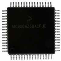
MC908AZ60ACFUER Freescale Semiconductor, MC908AZ60ACFUER Datasheet - Page 210

MC908AZ60ACFUER
Manufacturer Part Number
MC908AZ60ACFUER
Description
IC MCU 60K FLASH 8.4MHZ 64-QFP
Manufacturer
Freescale Semiconductor
Series
HC08r
Datasheet
1.MC908AZ60ACFUER.pdf
(414 pages)
Specifications of MC908AZ60ACFUER
Core Processor
HC08
Core Size
8-Bit
Speed
8.4MHz
Connectivity
CAN, SCI, SPI
Peripherals
LVD, POR, PWM
Number Of I /o
52
Program Memory Size
60KB (60K x 8)
Program Memory Type
FLASH
Eeprom Size
1K x 8
Ram Size
2K x 8
Voltage - Supply (vcc/vdd)
4.5 V ~ 5.5 V
Data Converters
A/D 15x8b
Oscillator Type
Internal
Operating Temperature
-40°C ~ 85°C
Package / Case
64-QFP
Processor Series
HC08AZ
Core
HC08
Data Bus Width
8 bit
Data Ram Size
2 KB
Interface Type
SCI, SPI
Maximum Clock Frequency
8.4 MHz
Number Of Programmable I/os
52
Number Of Timers
8
Maximum Operating Temperature
+ 85 C
Mounting Style
SMD/SMT
Development Tools By Supplier
FSICEBASE, M68CBL05CE, ZK-HC08AX-A, M68EM08AS/AZ60AE
Minimum Operating Temperature
- 40 C
On-chip Adc
8 bit, 15 Channel
Controller Family/series
HC08
No. Of I/o's
52
Eeprom Memory Size
1KB
Ram Memory Size
2KB
Cpu Speed
8MHz
No. Of Timers
2
Rohs Compliant
Yes
Lead Free Status / RoHS Status
Lead free / RoHS Compliant
Other names
MC908AZ60ACFUERTR
Available stocks
Company
Part Number
Manufacturer
Quantity
Price
Company:
Part Number:
MC908AZ60ACFUER
Manufacturer:
FREESCALE
Quantity:
5 560
Company:
Part Number:
MC908AZ60ACFUER
Manufacturer:
Freescale Semiconductor
Quantity:
10 000
- Current page: 210 of 414
- Download datasheet (5Mb)
Serial Peripheral Interface (SPI)
19.5.2 Transmission Format When CPHA = 0
Figure 19-4
as a replacement for data sheet parametric information. Two waveforms are shown for SCK: one for
CPOL = 0 and another for CPOL = 1. The diagram may be interpreted as a master or slave timing
diagram since the serial clock (SCK), master in/slave out (MISO), and master out/slave in (MOSI) pins
are directly connected between the master and the slave. The MISO signal is the output from the slave,
and the MOSI signal is the output from the master. The SS line is the slave select input to the slave. The
slave SPI drives its MISO output only when its slave select input (SS) is low, so that only the selected
slave drives to the master. The SS pin of the master is not shown but is assumed to be inactive. The SS
pin of the master must be high or must be reconfigured as general-purpose I/O not affecting the SPI (see
19.6.2 Mode Fault
the slave must begin driving its data before the first SPSCK edge, and a falling edge on the SS pin is used
to start the transmission. The SS pin must be toggled high and then low again between each byte
transmitted.
210
CAPTURE STROBE
FOR REFERENCE
FROM MASTER
SCK CPOL = 0
SCK CPOL = 1
SCK CYCLE #
FROM SLAVE
SS TO SLAVE
shows an SPI transmission in which CPHA (SPCR) is logic 0. The figure should not be used
MOSI
MISO
MC68HC908AZ60A • MC68HC908AS60A • MC68HC908AS60E Data Sheet, Rev. 6
Error). When CPHA = 0, the first SPSCK edge is the MSB capture strobe. Therefore,
MSB
Figure 19-4. Transmission Format (CPHA = 0)
MSB
1
BIT 6
BIT 6
2
BIT 5
BIT 5
3
BIT 4
BIT 4
4
BIT 3
BIT 3
5
BIT 2
BIT 2
6
BIT 1
BIT 1
7
Freescale Semiconductor
LSB
LSB
8
Related parts for MC908AZ60ACFUER
Image
Part Number
Description
Manufacturer
Datasheet
Request
R
Part Number:
Description:
Manufacturer:
Freescale Semiconductor, Inc
Datasheet:
Part Number:
Description:
Manufacturer:
Freescale Semiconductor, Inc
Datasheet:
Part Number:
Description:
Manufacturer:
Freescale Semiconductor, Inc
Datasheet:
Part Number:
Description:
Manufacturer:
Freescale Semiconductor, Inc
Datasheet:
Part Number:
Description:
Manufacturer:
Freescale Semiconductor, Inc
Datasheet:
Part Number:
Description:
Manufacturer:
Freescale Semiconductor, Inc
Datasheet:
Part Number:
Description:
Manufacturer:
Freescale Semiconductor, Inc
Datasheet:
Part Number:
Description:
Manufacturer:
Freescale Semiconductor, Inc
Datasheet:
Part Number:
Description:
Manufacturer:
Freescale Semiconductor, Inc
Datasheet:
Part Number:
Description:
Manufacturer:
Freescale Semiconductor, Inc
Datasheet:
Part Number:
Description:
Manufacturer:
Freescale Semiconductor, Inc
Datasheet:
Part Number:
Description:
Manufacturer:
Freescale Semiconductor, Inc
Datasheet:
Part Number:
Description:
Manufacturer:
Freescale Semiconductor, Inc
Datasheet:
Part Number:
Description:
Manufacturer:
Freescale Semiconductor, Inc
Datasheet:
Part Number:
Description:
Manufacturer:
Freescale Semiconductor, Inc
Datasheet:


