MC908AZ60ACFUER Freescale Semiconductor, MC908AZ60ACFUER Datasheet - Page 7
MC908AZ60ACFUER
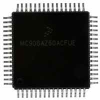
Manufacturer Part Number
MC908AZ60ACFUER
Description
IC MCU 60K FLASH 8.4MHZ 64-QFP
Manufacturer
Freescale Semiconductor
Series
HC08r
Datasheet
1.MC908AZ60ACFUER.pdf
(414 pages)
Specifications of MC908AZ60ACFUER
Core Processor
HC08
Core Size
8-Bit
Speed
8.4MHz
Connectivity
CAN, SCI, SPI
Peripherals
LVD, POR, PWM
Number Of I /o
52
Program Memory Size
60KB (60K x 8)
Program Memory Type
FLASH
Eeprom Size
1K x 8
Ram Size
2K x 8
Voltage - Supply (vcc/vdd)
4.5 V ~ 5.5 V
Data Converters
A/D 15x8b
Oscillator Type
Internal
Operating Temperature
-40°C ~ 85°C
Package / Case
64-QFP
Processor Series
HC08AZ
Core
HC08
Data Bus Width
8 bit
Data Ram Size
2 KB
Interface Type
SCI, SPI
Maximum Clock Frequency
8.4 MHz
Number Of Programmable I/os
52
Number Of Timers
8
Maximum Operating Temperature
+ 85 C
Mounting Style
SMD/SMT
Development Tools By Supplier
FSICEBASE, M68CBL05CE, ZK-HC08AX-A, M68EM08AS/AZ60AE
Minimum Operating Temperature
- 40 C
On-chip Adc
8 bit, 15 Channel
Controller Family/series
HC08
No. Of I/o's
52
Eeprom Memory Size
1KB
Ram Memory Size
2KB
Cpu Speed
8MHz
No. Of Timers
2
Rohs Compliant
Yes
Lead Free Status / RoHS Status
Lead free / RoHS Compliant
Other names
MC908AZ60ACFUERTR
Available stocks
Company
Part Number
Manufacturer
Quantity
Price
Company:

Part Number:
MC908AZ60ACFUER
Manufacturer:
FREESCALE
Quantity:
5 560
Company:
Part Number:
MC908AZ60ACFUER
Manufacturer:
Freescale Semiconductor
Quantity:
10 000


Table of Contents
1.1
1.2
1.3
1.4
1.4.1
1.4.2
1.4.3
1.4.4
1.4.5
1.4.6
1.4.7
1.4.8
1.4.9
1.4.10
1.4.11
1.4.12
1.4.13
1.4.14
1.4.15
1.4.16
1.4.17
1.4.18
1.4.19
1.4.20
1.4.21
1.4.22
1.5
2.1
2.2
2.3
2.4
3.1
3.2
Freescale Semiconductor
Introduction . . . . . . . . . . . . . . . . . . . . . . . . . . . . . . . . . . . . . . . . . . . . . . . . . . . . . . . . . . . . . . . . 21
Features. . . . . . . . . . . . . . . . . . . . . . . . . . . . . . . . . . . . . . . . . . . . . . . . . . . . . . . . . . . . . . . . . . . 21
MCU Block Diagram . . . . . . . . . . . . . . . . . . . . . . . . . . . . . . . . . . . . . . . . . . . . . . . . . . . . . . . . . 22
Pin Assignments . . . . . . . . . . . . . . . . . . . . . . . . . . . . . . . . . . . . . . . . . . . . . . . . . . . . . . . . . . . . 25
Ordering Information . . . . . . . . . . . . . . . . . . . . . . . . . . . . . . . . . . . . . . . . . . . . . . . . . . . . . . . . . 34
Introduction . . . . . . . . . . . . . . . . . . . . . . . . . . . . . . . . . . . . . . . . . . . . . . . . . . . . . . . . . . . . . . . . 35
I/O Section . . . . . . . . . . . . . . . . . . . . . . . . . . . . . . . . . . . . . . . . . . . . . . . . . . . . . . . . . . . . . . . . . 39
Additional Status and Control Registers . . . . . . . . . . . . . . . . . . . . . . . . . . . . . . . . . . . . . . . . . . 44
Vector Addresses and Priority . . . . . . . . . . . . . . . . . . . . . . . . . . . . . . . . . . . . . . . . . . . . . . . . . . 46
Introduction . . . . . . . . . . . . . . . . . . . . . . . . . . . . . . . . . . . . . . . . . . . . . . . . . . . . . . . . . . . . . . . . 49
Functional Description . . . . . . . . . . . . . . . . . . . . . . . . . . . . . . . . . . . . . . . . . . . . . . . . . . . . . . . . 49
Power Supply Pins (V
Oscillator Pins (OSC1 and OSC2) . . . . . . . . . . . . . . . . . . . . . . . . . . . . . . . . . . . . . . . . . . . . 28
External Reset Pin (RST). . . . . . . . . . . . . . . . . . . . . . . . . . . . . . . . . . . . . . . . . . . . . . . . . . . 28
External Interrupt Pin (IRQ) . . . . . . . . . . . . . . . . . . . . . . . . . . . . . . . . . . . . . . . . . . . . . . . . . 28
Analog Power Supply Pin (V
Analog Ground Pin (V
External Filter Capacitor Pin (CGMXFC) . . . . . . . . . . . . . . . . . . . . . . . . . . . . . . . . . . . . . . . 29
ADC Analog Power Supply Pin (V
ADC Analog Ground Pin (A
ADC Reference High Voltage Pin (V
Port A Input/Output (I/O) Pins (PTA7–PTA0). . . . . . . . . . . . . . . . . . . . . . . . . . . . . . . . . . . . 29
Port B I/O Pins (PTB7/ATD7–PTB0/ATD0) . . . . . . . . . . . . . . . . . . . . . . . . . . . . . . . . . . . . . 29
Port C I/O Pins (PTC5–PTC0) . . . . . . . . . . . . . . . . . . . . . . . . . . . . . . . . . . . . . . . . . . . . . . . 29
Port D I/O Pins (PTD7–PTD0/ATD8) . . . . . . . . . . . . . . . . . . . . . . . . . . . . . . . . . . . . . . . . . . 29
Port E I/O Pins (PTE7/SPSCK–PTE0/TxD) . . . . . . . . . . . . . . . . . . . . . . . . . . . . . . . . . . . . . 30
Port F I/O Pins (PTF6–PTF0/TACH2) . . . . . . . . . . . . . . . . . . . . . . . . . . . . . . . . . . . . . . . . . 30
Port G I/O Pins (PTG2/KBD2–PTG0/KBD0) . . . . . . . . . . . . . . . . . . . . . . . . . . . . . . . . . . . . 30
Port H I/O Pins (PTH1/KBD4–PTH0/KBD3). . . . . . . . . . . . . . . . . . . . . . . . . . . . . . . . . . . . . 30
CAN Transmit Pin (CANTx) . . . . . . . . . . . . . . . . . . . . . . . . . . . . . . . . . . . . . . . . . . . . . . . . . 30
CAN Receive Pin (CANRx) . . . . . . . . . . . . . . . . . . . . . . . . . . . . . . . . . . . . . . . . . . . . . . . . . 30
BDLC Transmit Pin (BDTxD) . . . . . . . . . . . . . . . . . . . . . . . . . . . . . . . . . . . . . . . . . . . . . . . . 30
BDLC Receive Pin (BDRxD) . . . . . . . . . . . . . . . . . . . . . . . . . . . . . . . . . . . . . . . . . . . . . . . . 30
MC68HC908AZ60A • MC68HC908AS60A • MC68HC908AS60E Data Sheet, Rev. 6
DD
SSA
Random-Access Memory (RAM)
and V
) . . . . . . . . . . . . . . . . . . . . . . . . . . . . . . . . . . . . . . . . . . . . . . . . . . 29
VSS/
DDA
General Description
SS
V
). . . . . . . . . . . . . . . . . . . . . . . . . . . . . . . . . . . . . . . . . . . . . 29
REFL
Memory Map
). . . . . . . . . . . . . . . . . . . . . . . . . . . . . . . . . . . . . . . . . . . . 28
DDAREF
Chapter 1
Chapter 2
Chapter 3
REFH
) . . . . . . . . . . . . . . . . . . . . . . . . . . . . . . . . . . . . . . . . 29
). . . . . . . . . . . . . . . . . . . . . . . . . . . . . . . . . . . . . . 29
) . . . . . . . . . . . . . . . . . . . . . . . . . . . . . . . . . . . . . 29
7
Related parts for MC908AZ60ACFUER
Image
Part Number
Description
Manufacturer
Datasheet
Request
R

Part Number:
Description:
Manufacturer:
Freescale Semiconductor, Inc
Datasheet:
Part Number:
Description:
Manufacturer:
Freescale Semiconductor, Inc
Datasheet:
Part Number:
Description:
Manufacturer:
Freescale Semiconductor, Inc
Datasheet:
Part Number:
Description:
Manufacturer:
Freescale Semiconductor, Inc
Datasheet:
Part Number:
Description:
Manufacturer:
Freescale Semiconductor, Inc
Datasheet:
Part Number:
Description:
Manufacturer:
Freescale Semiconductor, Inc
Datasheet:
Part Number:
Description:
Manufacturer:
Freescale Semiconductor, Inc
Datasheet:
Part Number:
Description:
Manufacturer:
Freescale Semiconductor, Inc
Datasheet:
Part Number:
Description:
Manufacturer:
Freescale Semiconductor, Inc
Datasheet:
Part Number:
Description:
Manufacturer:
Freescale Semiconductor, Inc
Datasheet:
Part Number:
Description:
Manufacturer:
Freescale Semiconductor, Inc
Datasheet:
Part Number:
Description:
Manufacturer:
Freescale Semiconductor, Inc
Datasheet:
Part Number:
Description:
Manufacturer:
Freescale Semiconductor, Inc
Datasheet:
Part Number:
Description:
Manufacturer:
Freescale Semiconductor, Inc
Datasheet:
Part Number:
Description:
Manufacturer:
Freescale Semiconductor, Inc
Datasheet: