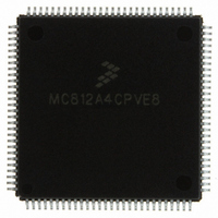
MC812A4CPVE8 Freescale Semiconductor, MC812A4CPVE8 Datasheet - Page 169

MC812A4CPVE8
Manufacturer Part Number
MC812A4CPVE8
Description
IC MCU 16BIT EEPROM 4K 112-LQFP
Manufacturer
Freescale Semiconductor
Series
HC12r
Datasheet
1.MC812A4CPVE8.pdf
(242 pages)
Specifications of MC812A4CPVE8
Core Processor
CPU12
Core Size
16-Bit
Speed
8MHz
Connectivity
SCI, SPI
Peripherals
POR, WDT
Number Of I /o
83
Program Memory Size
4KB (4K x 8)
Program Memory Type
EEPROM
Ram Size
1K x 8
Voltage - Supply (vcc/vdd)
4.5 V ~ 5.5 V
Data Converters
A/D 8x8b
Oscillator Type
Internal
Operating Temperature
-40°C ~ 85°C
Package / Case
112-LQFP
Processor Series
HC812A
Core
HC12
Data Bus Width
16 bit
Data Ram Size
1 KB
Interface Type
SCI, SPI
Maximum Clock Frequency
8 MHz
Number Of Programmable I/os
91
Number Of Timers
8
Maximum Operating Temperature
+ 85 C
Mounting Style
SMD/SMT
Minimum Operating Temperature
- 40 C
On-chip Adc
8 bit, 8 Channel
Controller Family/series
68HC12
No. Of I/o's
91
Eeprom Memory Size
4KB
Ram Memory Size
1KB
Cpu Speed
8MHz
No. Of Timers
1
Rohs Compliant
Yes
Lead Free Status / RoHS Status
Lead free / RoHS Compliant
Eeprom Size
-
Lead Free Status / Rohs Status
Details
Available stocks
Company
Part Number
Manufacturer
Quantity
Price
Company:
Part Number:
MC812A4CPVE8
Manufacturer:
MOTOLOLA
Quantity:
672
Company:
Part Number:
MC812A4CPVE8
Manufacturer:
Freescale Semiconductor
Quantity:
10 000
Part Number:
MC812A4CPVE8
Manufacturer:
NXP/恩智浦
Quantity:
20 000
Company:
Part Number:
MC812A4CPVE80
Manufacturer:
SHARP
Quantity:
5 510
14.6.2 SCI Control Register 1
Read: Anytime
Write: Anytime
LOOPS — Loop Select Bit
WOMS — Wired-OR Mode Select Bit
RSRC — Receiver Source Bit
Freescale Semiconductor
LOOPS
LOOPS enables loop operation. In loop operation the RXD pin is disconnected from the SCI, and the
transmitter output goes into the receiver input. Both the transmitter and the receiver must be enabled
to use the loop function.
The receiver input is determined by the RSRC bit. The transmitter output is controlled by the
associated DDRS bit.
If the data direction bit for the TXD pin is set and LOOPS = 1, the transmitter output appears on the
TXD pin. If the DDRS bit is clear and LOOPS = 1, the TXD pin is idle (high) if RSRC = 0 and
high-impedance if RSRC = 1. See
WOMS configures the TXD and RXD pins for open-drain operation. WOMS allows TXD pins to be tied
together in a multiple-transmitter system. Then the TXD pins of non-active transmitters follow the logic
level of an active 1. WOMS also affects the TXD and RXD pins when they are general-purpose outputs.
External pullup resistors are necessary on open-drain outputs.
When LOOPS = 1, the RSRC bit determines the internal feedback path for the receiver.
0
1
1
1
1 = Loop operation enabled
0 = Normal operation enabled
1 = TXD and RXD pins, open-drain when outputs
0 = TXD and RXD pins, full CMOS drive capability
1 = Receiver input connected to TXD pin
0 = Receiver input internally connected to transmitter output
RSRC
Reset:
Read:
Write:
SCI0: $00C2
SCI1: $00CA
X
0
0
0
LOOPS
Figure 14-19. SCI Control Register 1 (SC0CR1 or SC1CR1)
Bit 7
DDRSx
0
X
0
1
1
(1)
WOMS
6
0
Table 14-7. Loop Mode Functions
WOMS
MC68HC812A4 Data Sheet, Rev. 7
Table
X
X
0
1
RSRC
5
0
14-7.
Normal operation
Loop mode; transmitter output connected to receiver input
TXD pin disconnected
Loop mode; transmitter output connected to receiver input
TXD is CMOS output
Loop mode; transmitter output connected to receiver input
TXD is open-drain output
M
4
0
WAKE
3
0
Register Descriptions and Reset Initialization
Function of TXD Pin
ILT
2
0
PE
1
0
Bit 0
PT
0
169


