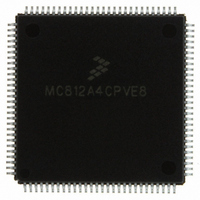
MC812A4CPVE8 Freescale Semiconductor, MC812A4CPVE8 Datasheet - Page 69

MC812A4CPVE8
Manufacturer Part Number
MC812A4CPVE8
Description
IC MCU 16BIT EEPROM 4K 112-LQFP
Manufacturer
Freescale Semiconductor
Series
HC12r
Datasheet
1.MC812A4CPVE8.pdf
(242 pages)
Specifications of MC812A4CPVE8
Core Processor
CPU12
Core Size
16-Bit
Speed
8MHz
Connectivity
SCI, SPI
Peripherals
POR, WDT
Number Of I /o
83
Program Memory Size
4KB (4K x 8)
Program Memory Type
EEPROM
Ram Size
1K x 8
Voltage - Supply (vcc/vdd)
4.5 V ~ 5.5 V
Data Converters
A/D 8x8b
Oscillator Type
Internal
Operating Temperature
-40°C ~ 85°C
Package / Case
112-LQFP
Processor Series
HC812A
Core
HC12
Data Bus Width
16 bit
Data Ram Size
1 KB
Interface Type
SCI, SPI
Maximum Clock Frequency
8 MHz
Number Of Programmable I/os
91
Number Of Timers
8
Maximum Operating Temperature
+ 85 C
Mounting Style
SMD/SMT
Minimum Operating Temperature
- 40 C
On-chip Adc
8 bit, 8 Channel
Controller Family/series
68HC12
No. Of I/o's
91
Eeprom Memory Size
4KB
Ram Memory Size
1KB
Cpu Speed
8MHz
No. Of Timers
1
Rohs Compliant
Yes
Lead Free Status / RoHS Status
Lead free / RoHS Compliant
Eeprom Size
-
Lead Free Status / Rohs Status
Details
Available stocks
Company
Part Number
Manufacturer
Quantity
Price
Company:
Part Number:
MC812A4CPVE8
Manufacturer:
MOTOLOLA
Quantity:
672
Company:
Part Number:
MC812A4CPVE8
Manufacturer:
Freescale Semiconductor
Quantity:
10 000
Part Number:
MC812A4CPVE8
Manufacturer:
NXP/恩智浦
Quantity:
20 000
Company:
Part Number:
MC812A4CPVE80
Manufacturer:
SHARP
Quantity:
5 510
6.3.11 Port E Assignment Register
Read: Anytime, if register is in the map
Write: Varies from bit to bit if register is in the map
The PEAR register selects between the general-purpose I/O functions and the alternate bus-control
functions of port E. The alternate bus-control functions override the associated DDRE bits.
The reset condition of this register depends on the mode of operation.
In peripheral mode, the PEAR register is not accessible for reads or writes. However, the PLLTE control
bit is cleared to configure PE6 as a test output from the PLL module.
ARSIE — Auxiliary Reset Input Enable Bit
PLLTE — PLL Testing Enable Bit
Freescale Semiconductor
•
•
•
•
Write anytime.
Normal modes: Write never
Special modes: Write anytime except the first time
1 = PE7 is a high-true reset input; reset timing is the same as that of the low-true RESET pin.
0 = PE7 is general-purpose I/O.
1 = PE6 is a test signal output from the PLL module (no effect in single-chip or normal expanded
0 = PE6 is general-purpose I/O or pipe output.
In normal single-chip mode, port E is general-purpose I/O.
In special single-chip mode, the E-clock is enabled as a timing reference, and the rest of port E is
general-purpose I/O.
In normal expanded modes, the E-clock is configured for its alternate bus-control function, and the
other bits of port E are general-purpose I/O. The reset vector is located in external memory and the
E-clock may be required for this access. If R/W is needed for external writable resources, PEAR
can be written during normal expanded modes.
In special expanded modes, IPIPE1, IPIPE0, E, R/W, and LSTRB are configured as bus-control
signals.
Special expanded narrow:
Normal expanded narrow:
Special expanded wide:
Normal expanded wide:
modes); PIPOE = 1 overrides this function and forces PE6 to be a pipe status output signal.
Special single-chip:
Normal single-chip
Peripheral:
Address: $000A
Reset:
Read:
Write:
Figure 6-11. Port E Assignment Register (PEAR)
ARSIE
Bit 7
0
0
0
0
0
0
0
PLLTE
MC68HC812A4 Data Sheet, Rev. 7
6
0
0
1
0
0
0
0
PIPOE
5
1
1
0
1
0
0
0
NECLK
4
0
0
1
0
1
0
0
LSTRE
3
1
1
0
1
0
0
0
RDWE
2
1
1
0
1
0
0
0
1
0
0
0
0
0
0
0
0
Bit 0
0
0
0
0
0
0
0
0
Registers
69


