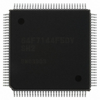
HD64F7144F50V Renesas Electronics America, HD64F7144F50V Datasheet - Page 33

HD64F7144F50V
Manufacturer Part Number
HD64F7144F50V
Description
IC SUPERH MCU FLASH 256K 112QFP
Manufacturer
Renesas Electronics America
Series
SuperH® SH7144r
Specifications of HD64F7144F50V
Core Processor
SH-2
Core Size
32-Bit
Speed
50MHz
Connectivity
EBI/EMI, I²C, SCI
Peripherals
DMA, POR, PWM, WDT
Number Of I /o
74
Program Memory Size
256KB (256K x 8)
Program Memory Type
FLASH
Ram Size
8K x 8
Voltage - Supply (vcc/vdd)
3 V ~ 3.6 V
Data Converters
A/D 8x10b
Oscillator Type
Internal
Operating Temperature
-20°C ~ 75°C
Package / Case
112-QFP
For Use With
HS0005KCU11H - EMULATOR E10A-USB H8S(X),SH2(A)EDK7145 - DEV EVALUATION KIT SH7145
Lead Free Status / RoHS Status
Lead free / RoHS Compliant
Eeprom Size
-
Available stocks
Company
Part Number
Manufacturer
Quantity
Price
Company:
Part Number:
HD64F7144F50V
Manufacturer:
RENESAS
Quantity:
450
Company:
Part Number:
HD64F7144F50V
Manufacturer:
Renesas Electronics America
Quantity:
10 000
Part Number:
HD64F7144F50V
Manufacturer:
RENESAS/瑞萨
Quantity:
20 000
- Current page: 33 of 932
- Download datasheet (6Mb)
Section 12 Watchdog Timer (WDT)
Figure 12.1 Block Diagram of WDT ..........................................................................................380
Figure 12.2 Operation in Watchdog Timer Mode.......................................................................386
Figure 12.3 Operation in Interval Timer Mode...........................................................................386
Figure 12.4 Timing of Setting OVF............................................................................................387
Figure 12.5 Timing of Setting WOVF ........................................................................................388
Figure 12.6 Writing to TCNT and TCSR ...................................................................................389
Figure 12.7 Writing to RSTCSR.................................................................................................390
Figure 12.8 Contention between TCNT Write and Increment....................................................390
Figure 12.9 Example of System Reset Circuit Using WDTOVF Signal ....................................391
Section 13 Serial Communication Interface (SCI)
Figure 13.1 Block Diagram of SCI .............................................................................................394
Figure 13.2 Data Format in Asynchronous Communication
Figure 13.3 Receive Data Sampling Timing in Asynchronous Mode ........................................428
Figure 13.4 Relation between Output Clock and Transmit Data Phase
Figure 13.5 Sample SCI Initialization Flowchart .......................................................................430
Figure 13.6 Example of Operation in Transmission in Asynchronous Mode
Figure 13.7 Sample Serial Transmission Flowchart ...................................................................432
Figure 13.8 Example of SCI Operation in Reception (Example with 8-Bit Data, Parity,
Figure 13.9 Sample Serial Reception Data Flowchart (1) ..........................................................435
Figure 13.9 Sample Serial Reception Data Flowchart (2) ..........................................................436
Figure 13.10 Example of Communication Using Multiprocessor Format
Figure 13.11 Sample Multiprocessor Serial Transmission Flowchart ........................................439
Figure 13.12 Example of SCI Operation in Reception (Example with 8-Bit Data,
Figure 13.13 Sample Multiprocessor Serial Reception Flowchart (1) ........................................441
Figure 13.13 Sample Multiprocessor Serial Reception Flowchart (2) ........................................442
Figure 13.14 Data Format in Clocked Synchronous Communication (For LSB-First) ..............443
Figure 13.15 Sample SCI Initialization Flowchart .....................................................................444
Figure 13.16 Sample SCI Transmission Operation in Clocked Synchronous Mode ..................446
Figure 13.17 Sample Serial Transmission Flowchart .................................................................446
Figure 13.18 Example of SCI Operation in Reception ...............................................................447
Figure 13.19 Sample Serial Reception Flowchart.......................................................................448
Figure 13.20 Sample Flowchart of Simultaneous Serial Transmit and Receive Operations.......450
Figure 13.21 Example of Pin Connections for Smart Card Interface .........................................451
(Example with 8-Bit Data, Parity, Two Stop Bits) ..................................................426
(Asynchronous Mode) .............................................................................................429
(Example with 8-Bit Data, Parity, One Stop Bit).....................................................431
One Stop Bit) ...........................................................................................................433
(Transmission of Data H'AA to Receiving Station A) ..........................................438
Multiprocessor Bit, One Stop Bit) .........................................................................440
Rev.4.00 Mar. 27, 2008, Page xxxi of xliv
REJ09B0108-0400
Related parts for HD64F7144F50V
Image
Part Number
Description
Manufacturer
Datasheet
Request
R

Part Number:
Description:
KIT STARTER FOR M16C/29
Manufacturer:
Renesas Electronics America
Datasheet:

Part Number:
Description:
KIT STARTER FOR R8C/2D
Manufacturer:
Renesas Electronics America
Datasheet:

Part Number:
Description:
R0K33062P STARTER KIT
Manufacturer:
Renesas Electronics America
Datasheet:

Part Number:
Description:
KIT STARTER FOR R8C/23 E8A
Manufacturer:
Renesas Electronics America
Datasheet:

Part Number:
Description:
KIT STARTER FOR R8C/25
Manufacturer:
Renesas Electronics America
Datasheet:

Part Number:
Description:
KIT STARTER H8S2456 SHARPE DSPLY
Manufacturer:
Renesas Electronics America
Datasheet:

Part Number:
Description:
KIT STARTER FOR R8C38C
Manufacturer:
Renesas Electronics America
Datasheet:

Part Number:
Description:
KIT STARTER FOR R8C35C
Manufacturer:
Renesas Electronics America
Datasheet:

Part Number:
Description:
KIT STARTER FOR R8CL3AC+LCD APPS
Manufacturer:
Renesas Electronics America
Datasheet:

Part Number:
Description:
KIT STARTER FOR RX610
Manufacturer:
Renesas Electronics America
Datasheet:

Part Number:
Description:
KIT STARTER FOR R32C/118
Manufacturer:
Renesas Electronics America
Datasheet:

Part Number:
Description:
KIT DEV RSK-R8C/26-29
Manufacturer:
Renesas Electronics America
Datasheet:

Part Number:
Description:
KIT STARTER FOR SH7124
Manufacturer:
Renesas Electronics America
Datasheet:

Part Number:
Description:
KIT STARTER FOR H8SX/1622
Manufacturer:
Renesas Electronics America
Datasheet:


