HD64F7144F50V Renesas Electronics America, HD64F7144F50V Datasheet - Page 53
HD64F7144F50V
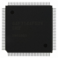
Manufacturer Part Number
HD64F7144F50V
Description
IC SUPERH MCU FLASH 256K 112QFP
Manufacturer
Renesas Electronics America
Series
SuperH® SH7144r
Specifications of HD64F7144F50V
Core Processor
SH-2
Core Size
32-Bit
Speed
50MHz
Connectivity
EBI/EMI, I²C, SCI
Peripherals
DMA, POR, PWM, WDT
Number Of I /o
74
Program Memory Size
256KB (256K x 8)
Program Memory Type
FLASH
Ram Size
8K x 8
Voltage - Supply (vcc/vdd)
3 V ~ 3.6 V
Data Converters
A/D 8x10b
Oscillator Type
Internal
Operating Temperature
-20°C ~ 75°C
Package / Case
112-QFP
For Use With
HS0005KCU11H - EMULATOR E10A-USB H8S(X),SH2(A)EDK7145 - DEV EVALUATION KIT SH7145
Lead Free Status / RoHS Status
Lead free / RoHS Compliant
Eeprom Size
-
Available stocks
Company
Part Number
Manufacturer
Quantity
Price
Company:

Part Number:
HD64F7144F50V
Manufacturer:
RENESAS
Quantity:
450
Company:
Part Number:
HD64F7144F50V
Manufacturer:
Renesas Electronics America
Quantity:
10 000
Part Number:
HD64F7144F50V
Manufacturer:
RENESAS/瑞萨
Quantity:
20 000


PE3/TIOC0D/DRAK1/AUDATA3*
PE2/TIOC0C/DREQ1/AUDRST*
PE4/TIOC1A/RXD3/AUDATA2*
PE5/TIOC1B/TXD3/AUDATA1*
PE6/TIOC2A/SCK3/AUDATA0*
PE0/TIOC0A/DREQ0/AUDCK*
PE1/TIOC0B/DRAK0/AUDMD*
PE11/TIOC3D/TDO*
PE9/TIOC3B/TRST*
PE12/TIOC4A/TCK*
PE8/TIOC3A/SCK2/TMS*
PE10/TIOC3C/TXD2/TDI*
ASEBRKAK Processing
Notes :
PA2/SCK0/DREQ0/IRQ0
PA5/SCK1/DREQ1/IRQ1
PE13/TIOC4B/MRES
Product type
Masked ROM version and ROM less version
F-ZTAT version (when using E10A)
F-ZTAT version (Not when using E10A)
PE7/TIOC2B/RXD2
1. Fixed as Vcc in the masked ROM version and ROM less version, and used as an FWP input pin in the F-ZTAT version (used as an FWE in
2. Used for E10A debugging mode. Used as an ASEBRKAK output pin in the F-ZTAT version. Refer to the table below for
3. Used for E10A debugging mode. Fixed to Vss in the masked ROM version and ROM less version, or used as a DBGMD input pin in the
4. Valid only in the F-ZTAT version (invalid only in the masked ROM version and ROM less version).
5. Valid only in the masked ROM version and ROM less version (invalid in the F-ZTAT version and emulator).
PA0/RXD0
PA3/RXD1
PA1/TXD0
PA4/TXD1
programmer mode).
processing the ASEBRKAK pin.
F-ZTAT version.
PF0/AN0
PF1/AN1
PF2/AN2
PF3/AN3
PF4/AN4
PF5/AN5
PF6/AN6
PF7/AN7
4
4
4
/SCK3
/RXD3
/TXD3
AVref
AVss
AVcc
Vcc
Vss
Vss
Vcc
Vss
4
4
4
4
4
4
4
4
4
109
110
111
112
113
114
115
116
117
118
119
120
121
122
123
124
125
126
127
128
129
130
131
132
133
134
135
136
137
138
139
140
141
142
143
144
108 107106 105 104 103102 101 100 99 98 97 96 95 94 93 92 91 90 89 88 87 86 85 84 83 82 81 80 79 78 77 76 75 74 73
1
2 3
4 5
Figure 1.4 SH7145 Pin Arrangement
6 7
8
Fixed to Vcc
Yes
No
Yes
9 10 11 12 13 14 15 16 17 18 19 20 21 22 23 24 25 26 27 28 29 30 31 32 33 34 35 36
Fixed to Vss
Yes
No
Yes
(Top view)
LQFP-144
Processing
Pull-up
Yes
Yes
Yes
Rev.4.00 Mar. 27, 2008 Page 7 of 882
Pull-down
Yes
No
Yes
REJ09B0108-0400
PD16/D16/IRQ0/AUDATA0*
Vss
PD17/D17/IRQ1/AUDATA1*
PD18/D18/IRQ2/AUDATA2*
PD19/D19/IRQ3/AUDATA3*
PD20/D20/IRQ4/AUDRST*
PD21/D21/IRQ5/AUDMD*
PD22/D22/IRQ6/AUDCK*
PD23/D23/IRQ7/AUDSYNC*
Vcc
PD24/D24/DERQ0
Vss
PD25/D25/DREQ1
PD26/D26/DACK0
PD27/D27/DACK1
PD28/D28/CS2
PD29/D29/CS3
Vss
PA6/TCLKA/CS2
PA7/TCLKB/CS3
PA8/TCLKC/IRQ2
PA9/TCLKD/IRQ3
PA10/CS0
PA11/CS1
PA12/WRL
PA13/WRH
PD30/D30/IRQOUT
PD31/D31/ADTRG
WDTOVF
PA14/RD
Vss(DBGMD*
PB9/IRQ7/A21/ADTRG
Vcc
PB8/IRQ6/A20/WAIT
PB7/IRQ5/A19/BREQ
PB6/IRQ4/A18/BACK
NC
No
No
No
1. Overview
3
)
4
4
4
4
4
4
4
4
Related parts for HD64F7144F50V
Image
Part Number
Description
Manufacturer
Datasheet
Request
R


Part Number:
Description:
KIT STARTER FOR M16C/29
Manufacturer:
Renesas Electronics America
Datasheet:

Part Number:
Description:
KIT STARTER FOR R8C/2D
Manufacturer:
Renesas Electronics America
Datasheet:

Part Number:
Description:
R0K33062P STARTER KIT
Manufacturer:
Renesas Electronics America
Datasheet:

Part Number:
Description:
KIT STARTER FOR R8C/23 E8A
Manufacturer:
Renesas Electronics America
Datasheet:

Part Number:
Description:
KIT STARTER FOR R8C/25
Manufacturer:
Renesas Electronics America
Datasheet:

Part Number:
Description:
KIT STARTER H8S2456 SHARPE DSPLY
Manufacturer:
Renesas Electronics America
Datasheet:

Part Number:
Description:
KIT STARTER FOR R8C38C
Manufacturer:
Renesas Electronics America
Datasheet:

Part Number:
Description:
KIT STARTER FOR R8C35C
Manufacturer:
Renesas Electronics America
Datasheet:

Part Number:
Description:
KIT STARTER FOR R8CL3AC+LCD APPS
Manufacturer:
Renesas Electronics America
Datasheet:
Part Number:
Description:
KIT STARTER FOR RX610
Manufacturer:
Renesas Electronics America
Datasheet:

Part Number:
Description:
KIT STARTER FOR R32C/118
Manufacturer:
Renesas Electronics America
Datasheet:

Part Number:
Description:
KIT DEV RSK-R8C/26-29
Manufacturer:
Renesas Electronics America
Datasheet:

Part Number:
Description:
KIT STARTER FOR SH7124
Manufacturer:
Renesas Electronics America
Datasheet:

Part Number:
Description:
KIT STARTER FOR H8SX/1622
Manufacturer:
Renesas Electronics America
Datasheet: