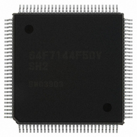
HD64F7144F50V Renesas Electronics America, HD64F7144F50V Datasheet - Page 376

HD64F7144F50V
Manufacturer Part Number
HD64F7144F50V
Description
IC SUPERH MCU FLASH 256K 112QFP
Manufacturer
Renesas Electronics America
Series
SuperH® SH7144r
Specifications of HD64F7144F50V
Core Processor
SH-2
Core Size
32-Bit
Speed
50MHz
Connectivity
EBI/EMI, I²C, SCI
Peripherals
DMA, POR, PWM, WDT
Number Of I /o
74
Program Memory Size
256KB (256K x 8)
Program Memory Type
FLASH
Ram Size
8K x 8
Voltage - Supply (vcc/vdd)
3 V ~ 3.6 V
Data Converters
A/D 8x10b
Oscillator Type
Internal
Operating Temperature
-20°C ~ 75°C
Package / Case
112-QFP
For Use With
HS0005KCU11H - EMULATOR E10A-USB H8S(X),SH2(A)EDK7145 - DEV EVALUATION KIT SH7145
Lead Free Status / RoHS Status
Lead free / RoHS Compliant
Eeprom Size
-
Available stocks
Company
Part Number
Manufacturer
Quantity
Price
Company:
Part Number:
HD64F7144F50V
Manufacturer:
RENESAS
Quantity:
450
Company:
Part Number:
HD64F7144F50V
Manufacturer:
Renesas Electronics America
Quantity:
10 000
Part Number:
HD64F7144F50V
Manufacturer:
RENESAS/瑞萨
Quantity:
20 000
- Current page: 376 of 932
- Download datasheet (6Mb)
11.
11.7.12 Counter Value during Complementary PWM Mode Stop
When counting operation is suspended with TCNT_3 and TCNT_4 in complementary PWM
mode, TCNT_3 has the timer dead time register (TDDR) value, and TCNT_4 is held at H'0000.
When restarting complementary PWM mode, counting begins automatically from the initialized
state. This explanatory diagram is shown in figure 11.80.
When counting begins in another operating mode, be sure that TCNT_3 and TCNT_4 are set to
the initial values.
11.7.13 Buffer Operation Setting in Complementary PWM Mode
In complementary PWM mode, conduct rewrites by buffer operation for the PWM cycle setting
register (TGRA_3), timer cycle data register (TCDR), and duty setting registers (TGRB_3,
TGRA_4, and TGRB_4).
In complementary PWM mode, channel 3 and channel 4 buffers operate in accordance with bit
settings BFA and BFB of TMDR_3. When TMDR_3’s BFA bit is set to 1, TGRC_3 functions as a
buffer register for TGRA_3. At the same time, TGRC_4 functions as the buffer register for
TGRA_4, while the TCBR functions as the TCDR’s buffer register.
Rev.4.00 Mar. 27, 2008 Page 330 of 882
REJ09B0108-0400
Multi-Function Timer Pulse Unit (MTU)
Figure 11.80
TGRA_3
TCDR
TDDR
H'0000
Complementary PWM
TCNT_3
Counter Value during Complementary PWM Mode Stop
mode operation
TCNT_4
Counter
operation stop
Complementary
PMW restart
Complementary PWM
mode operation
Related parts for HD64F7144F50V
Image
Part Number
Description
Manufacturer
Datasheet
Request
R

Part Number:
Description:
KIT STARTER FOR M16C/29
Manufacturer:
Renesas Electronics America
Datasheet:

Part Number:
Description:
KIT STARTER FOR R8C/2D
Manufacturer:
Renesas Electronics America
Datasheet:

Part Number:
Description:
R0K33062P STARTER KIT
Manufacturer:
Renesas Electronics America
Datasheet:

Part Number:
Description:
KIT STARTER FOR R8C/23 E8A
Manufacturer:
Renesas Electronics America
Datasheet:

Part Number:
Description:
KIT STARTER FOR R8C/25
Manufacturer:
Renesas Electronics America
Datasheet:

Part Number:
Description:
KIT STARTER H8S2456 SHARPE DSPLY
Manufacturer:
Renesas Electronics America
Datasheet:

Part Number:
Description:
KIT STARTER FOR R8C38C
Manufacturer:
Renesas Electronics America
Datasheet:

Part Number:
Description:
KIT STARTER FOR R8C35C
Manufacturer:
Renesas Electronics America
Datasheet:

Part Number:
Description:
KIT STARTER FOR R8CL3AC+LCD APPS
Manufacturer:
Renesas Electronics America
Datasheet:

Part Number:
Description:
KIT STARTER FOR RX610
Manufacturer:
Renesas Electronics America
Datasheet:

Part Number:
Description:
KIT STARTER FOR R32C/118
Manufacturer:
Renesas Electronics America
Datasheet:

Part Number:
Description:
KIT DEV RSK-R8C/26-29
Manufacturer:
Renesas Electronics America
Datasheet:

Part Number:
Description:
KIT STARTER FOR SH7124
Manufacturer:
Renesas Electronics America
Datasheet:

Part Number:
Description:
KIT STARTER FOR H8SX/1622
Manufacturer:
Renesas Electronics America
Datasheet:


