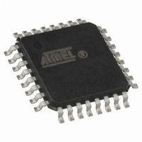
ATMEGA64M1-AU Atmel, ATMEGA64M1-AU Datasheet - Page 247

ATMEGA64M1-AU
Manufacturer Part Number
ATMEGA64M1-AU
Description
IC MCU AVR 64K FLASH 32TQFP
Manufacturer
Atmel
Series
AVR® ATmegar
Specifications of ATMEGA64M1-AU
Core Processor
AVR
Core Size
8-Bit
Speed
16MHz
Connectivity
CAN, LIN, SPI, UART/USART
Peripherals
Brown-out Detect/Reset, POR, PWM, Temp Sensor, WDT
Program Memory Size
64KB (32K x 16)
Program Memory Type
FLASH
Eeprom Size
2K x 8
Ram Size
4K x 8
Voltage - Supply (vcc/vdd)
2.7 V ~ 5.5 V
Data Converters
A/D 11x10b; D/A 1x10b
Oscillator Type
Internal
Operating Temperature
-40°C ~ 85°C
Package / Case
32-TQFP, 32-VQFP
Lead Free Status / RoHS Status
Lead free / RoHS Compliant
Number Of I /o
-
Lead Free Status / Rohs Status
Details
Available stocks
Company
Part Number
Manufacturer
Quantity
Price
- Current page: 247 of 341
- Download datasheet (6Mb)
21.10.8
8209D–AVR–11/10
AMP0CSR – Amplifier 0 Control and Status register
• Bit 6:0 – ADC10D..8D, ACMP0D, ACMP1D, ACMP3D, AMP0PD, AMP0ND, AMP1PD,
When this bit is written logic one, the digital input buffer on the corresponding ADC pin is dis-
abled. The corresponding PIN Register bit will always read as zero when this bit is set. When an
analog signal is applied to an analog pin and the digital input from this pin is not needed, this bit
should be written logic one to reduce power consumption in the digital input buffer.
Bit
Read/Write
Initial Value
• Bit 7 – AMP0EN: Amplifier 0 Enable Bit
Set this bit to enable the Amplifier 0.
Clear this bit to disable the Amplifier 0.
Clearing this bit while a conversion is running will take effect at the end of the conversion.
Warning: Always clear AMP0TS0:1 when clearing AMP0EN.
• Bit 6 – AMP0IS: Amplifier 0 Input Shunt
Set this bit to short-circuit the Amplifier 0 input.
Clear this bit to normally use the Amplifier 0.
• Bit 5:4 – AMP0G[1:0]: Amplifier 0 Gain Selection Bits
These 2 bits determine the gain of the amplifier 0.
The different setting are shown in
Table 21-8.
To ensure an accurate result, after the gain value has been changed, the amplifier input needs
to have a quite stable input value during at least 4 Amplifier synchronization clock periods.
• Bit 3 – AMPCMP0: Amplifier 0 - Comparator 0 connection
Set this bit to connect the amplifier 0 to the comparator 0 positive input. In this configuration the
comparator clock is adapted to the amplifier clock and AMP0TS[2:0] bits have no effect.
Clear this bit to normally use the Amplifier 0.
• Bit 2:0 – AMP0TS[2:0]: Amplifier 0 Clock Source Selection Bits
In accordance with the
the clock for the amplifier 0. This clock source is necessary to start the conversion on the ampli-
fied channel.
AMP0G[1:0]
AMP1ND, AMP2PD:
ADC10..8, ACMP0, ACMP1, ACMP3, AMP0P, AMP0N, AMP1P, AMP1N, AMP2P Digital
Input Disable
00
01
10
11
Amplifier 0 Gain Selection
AMP0EN
R/W
7
0
Table 21-9 on page
AMP0IS
R/W
6
0
AMP0G1
Table
R/W
5
0
21-8.
AMP0G0
248, these 3 bits select the event which will generate
R/W
4
0
ATmega16M1/32M1/64M1
AMPCMP0
Description
R/W
Gain 10
Gain 20
Gain 40
Gain 5
3
0
AMP0TS2
R/W
2
0
AMP0TS1
R/W
1
0
AMP0TS0
R/W
0
0
AMP0CSR
247
Related parts for ATMEGA64M1-AU
Image
Part Number
Description
Manufacturer
Datasheet
Request
R

Part Number:
Description:
Manufacturer:
Atmel Corporation
Datasheet:

Part Number:
Description:
Manufacturer:
ATMEL Corporation
Datasheet:

Part Number:
Description:
Manufacturer:
ATMEL Corporation
Datasheet:

Part Number:
Description:
IC AVR MCU 64K 16MHZ 5V 64TQFP
Manufacturer:
Atmel
Datasheet:

Part Number:
Description:
IC AVR MCU 64K 16MHZ 5V 64-QFN
Manufacturer:
Atmel
Datasheet:

Part Number:
Description:
IC AVR MCU 64K 16MHZ COM 64-TQFP
Manufacturer:
Atmel
Datasheet:

Part Number:
Description:
IC AVR MCU 64K 16MHZ IND 64-TQFP
Manufacturer:
Atmel
Datasheet:

Part Number:
Description:
IC AVR MCU 64K 16MHZ COM 64-QFN
Manufacturer:
Atmel
Datasheet:

Part Number:
Description:
MCU AVR 64KB FLASH 16MHZ 64TQFP
Manufacturer:
Atmel
Datasheet:

Part Number:
Description:
MCU AVR 64KB FLASH 16MHZ 64QFN
Manufacturer:
Atmel
Datasheet:

Part Number:
Description:
IC AVR MCU 64K 16MHZ IND 64-QFN
Manufacturer:
Atmel
Datasheet:

Part Number:
Description:
IC MCU AVR 64K 5V 16MHZ 64-TQFP
Manufacturer:
Atmel
Datasheet:

Part Number:
Description:
IC MCU AVR 64K 5V 16MHZ 64-QFN
Manufacturer:
Atmel
Datasheet:

Part Number:
Description:
MCU 8-Bit ATmega AVR RISC 64KB Flash 5V 64-Pin TQFP T/R
Manufacturer:
Atmel
Datasheet:


