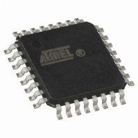
ATMEGA64M1-AU Atmel, ATMEGA64M1-AU Datasheet - Page 79

ATMEGA64M1-AU
Manufacturer Part Number
ATMEGA64M1-AU
Description
IC MCU AVR 64K FLASH 32TQFP
Manufacturer
Atmel
Series
AVR® ATmegar
Specifications of ATMEGA64M1-AU
Core Processor
AVR
Core Size
8-Bit
Speed
16MHz
Connectivity
CAN, LIN, SPI, UART/USART
Peripherals
Brown-out Detect/Reset, POR, PWM, Temp Sensor, WDT
Program Memory Size
64KB (32K x 16)
Program Memory Type
FLASH
Eeprom Size
2K x 8
Ram Size
4K x 8
Voltage - Supply (vcc/vdd)
2.7 V ~ 5.5 V
Data Converters
A/D 11x10b; D/A 1x10b
Oscillator Type
Internal
Operating Temperature
-40°C ~ 85°C
Package / Case
32-TQFP, 32-VQFP
Lead Free Status / RoHS Status
Lead free / RoHS Compliant
Number Of I /o
-
Lead Free Status / Rohs Status
Details
Available stocks
Company
Part Number
Manufacturer
Quantity
Price
- Current page: 79 of 341
- Download datasheet (6Mb)
ATmega16M1/32M1/64M1
ACMPN2, Analog Comparator 2 Negative Input. Configure the port pin as input with the internal
pull-up switched off to avoid the digital port function from interfering with the function of the Ana-
log Comparator.
INT0, External Interrupt source 0. This pin can serve as an external interrupt source to the MCU.
PCINT22, Pin Change Interrupt 23.
• ADC2/ACMP2/PCINT21 – Bit 5
ADC2, Analog to Digital Converter, input channel 2.
ACMP2, Analog Comparator 1 Positive Input. Configure the port pin as input with the internal
pull-up switched off to avoid the digital port function from interfering with the function of the Ana-
log Comparator.
PCINT21, Pin Change Interrupt 21.
• PCINT20/ADC1/RXD/RXLIN/ICP1/SCK_A – Bit 4
ADC1, Analog to Digital Converter, input channel 1.
RXD/RXLIN, LIN/UART Receive Pin. Receive Data (Data input pin for the LIN/UART). When the
LIN/UART receiver is enabled this pin is configured as an input regardless of the value of
DDRD4. When the UART forces this pin to be an input, a logical one in PORTD4 will turn on the
internal pull-up.
ICP1, Input Capture Pin1: This pin can act as an input capture pin for Timer/Counter1.
SCK_A: Master Clock output, Slave Clock input pin for SPI channel. When the SPI is enabled as
a slave, this pin is configured as an input regardless of the setting of DDD4. When the SPI is
enabled as a master, the data direction of this pin is controlled by DDD4. When the pin is forced
to be an input, the pull-up can still be controlled by the PORTD4 bit.
PCINT20, Pin Change Interrupt 20.
• PCINT19/TXD/TXLIN/OC0A/SS/MOSI_A, Bit 3
TXD/TXLIN, LIN/UART Transmit pin. Data output pin for the LIN/UART. When the LIN/UART
Transmitter is enabled, this pin is configured as an output regardless of the value of DDD3.
OC0A, Output Compare Match A output: This pin can serve as an external output for the
Timer/Counter0 Output Compare A. The pin has to be configured as an output (DDD3 set “one”)
to serve this function. The OC0A pin is also the output pin for the PWM mode.
SS: Slave Port Select input. When the SPI is enabled as a slave, this pin is configured as an
input regardless of the setting of DDD3. As a slave, the SPI is activated when this pin is driven
low. When the SPI is enabled as a master, the data direction of this pin is controlled by DDD3.
When the pin is forced to be an input, the pull-up can still be controlled by the PORTD3 bit.
MOSI_A: SPI Master Data output, Slave Data input for SPI channel. When the SPI is enabled as
a slave, this pin is configured as an input regardless of the setting of DDD3 When the SPI is
enabled as a master, the data direction of this pin is controlled by DDD3. When the pin is forced
to be an input, the pull-up can still be controlled by the PORTD3 bit.
PCINT19, Pin Change Interrupt 19.
79
8209D–AVR–11/10
Related parts for ATMEGA64M1-AU
Image
Part Number
Description
Manufacturer
Datasheet
Request
R

Part Number:
Description:
Manufacturer:
Atmel Corporation
Datasheet:

Part Number:
Description:
Manufacturer:
ATMEL Corporation
Datasheet:

Part Number:
Description:
Manufacturer:
ATMEL Corporation
Datasheet:

Part Number:
Description:
IC AVR MCU 64K 16MHZ 5V 64TQFP
Manufacturer:
Atmel
Datasheet:

Part Number:
Description:
IC AVR MCU 64K 16MHZ 5V 64-QFN
Manufacturer:
Atmel
Datasheet:

Part Number:
Description:
IC AVR MCU 64K 16MHZ COM 64-TQFP
Manufacturer:
Atmel
Datasheet:

Part Number:
Description:
IC AVR MCU 64K 16MHZ IND 64-TQFP
Manufacturer:
Atmel
Datasheet:

Part Number:
Description:
IC AVR MCU 64K 16MHZ COM 64-QFN
Manufacturer:
Atmel
Datasheet:

Part Number:
Description:
MCU AVR 64KB FLASH 16MHZ 64TQFP
Manufacturer:
Atmel
Datasheet:

Part Number:
Description:
MCU AVR 64KB FLASH 16MHZ 64QFN
Manufacturer:
Atmel
Datasheet:

Part Number:
Description:
IC AVR MCU 64K 16MHZ IND 64-QFN
Manufacturer:
Atmel
Datasheet:

Part Number:
Description:
IC MCU AVR 64K 5V 16MHZ 64-TQFP
Manufacturer:
Atmel
Datasheet:

Part Number:
Description:
IC MCU AVR 64K 5V 16MHZ 64-QFN
Manufacturer:
Atmel
Datasheet:

Part Number:
Description:
MCU 8-Bit ATmega AVR RISC 64KB Flash 5V 64-Pin TQFP T/R
Manufacturer:
Atmel
Datasheet:


