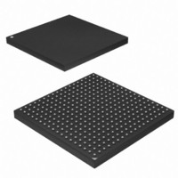
AT91SAM9G45-CU-999 Atmel, AT91SAM9G45-CU-999 Datasheet - Page 1108

AT91SAM9G45-CU-999
Manufacturer Part Number
AT91SAM9G45-CU-999
Description
IC MCU ARM9 APMC 324TFBGA
Manufacturer
Atmel
Series
AT91SAMr
Datasheet
1.AT91SAM9G45-EKES.pdf
(1218 pages)
Specifications of AT91SAM9G45-CU-999
Core Processor
ARM9
Core Size
16/32-Bit
Speed
400MHz
Connectivity
EBI/EMI, Ethernet, I²C, IrDA, MMC, SPI, SSC, UART/USART, USB
Peripherals
AC'97, DMA, I²S, LCD, POR, PWM, WDT
Number Of I /o
160
Program Memory Size
64KB (64K x 8)
Program Memory Type
ROM
Ram Size
128K x 8
Voltage - Supply (vcc/vdd)
0.9 V ~ 1.1 V
Data Converters
A/D 8x10b
Oscillator Type
Internal
Operating Temperature
-40°C ~ 85°C
Package / Case
324-TFBGA
Lead Free Status / RoHS Status
Lead free / RoHS Compliant
Eeprom Size
-
Lead Free Status / Rohs Status
Supplier Unconfirmed
Available stocks
Company
Part Number
Manufacturer
Quantity
Price
- Current page: 1108 of 1218
- Download datasheet (19Mb)
Table 45-13. Dithering Algorithm for Color Mode (Continued)
Note:
45.6.2.7
45.6.2.8
Figure 45-3. Full Frame Timing, MMODE=1, MVAL=1
1108
Frame
N+2
N+2
…
Ri = red pixel component ON. Gi = green pixel component ON. Bi = blue pixel component ON. ri = red pixel component OFF.
gi = green pixel component OFF. bi = blue pixel component OFF.
AT91SAM9G45
green_data_1
blue_data_1
Shifter
Timegen
Signal
…
The FIFO, Serializer, Palette and Dithering modules process one pixel at a time in monochrome
mode and three sub-pixels at a time in color mode (R,G,B components). This module packs the
data according to the output interface. This interface can be programmed in the DISTYPE,
SCANMOD, and IFWIDTH fields of the LDCCON3 register.
The DISTYPE field selects between TFT, STN monochrome and STN color display. The SCAN-
MODE field selects between single and dual scan modes; in TFT mode, only single scan is
supported. The IFWIDTH field configures the width of the interface in STN mode: 4-bit (in single
scan mode only), 8-bit and 16-bit (in dual scan mode only).
For a more detailed description of the fields, see
page
For a more detailed description of the LCD Interface, see
The time generator block generates the control signals LCDDOTCK, LCDHSYNC, LCDVSYNC,
LCDDEN, and LCDMOD, used by the LCD module. This block is programmable in order to sup-
port different types of LCD modules and obtain the output clock signals, which are derived from
the LCDC Core clock.
The LCDMOD signal provides an AC signal for the display. It is used by the LCD to alternate the
polarity of the row and column voltages used to turn the pixels on and off. This prevents the liq-
uid crystal from degradation. It can be configured to toggle every frame (bit MMODE = 0 in
LCDMVAL register) or to toggle every programmable number of LCDHSYNC pulses (bit
MMODE = 1, number of pulses defined in MVAL field of LCDMVAL register).
Figure 45-3
LCDDOTCK
LCDMOD
Shadow Level
LCDVSYNC
1125.
1010
1010
…
and
f
LCD_MOD
Figure 45-4 on page 1109
Line1
Line2
Bit used
Line3
…
3
2
=
Line4
--------------------------------------- -
2
f
Line5
LCD_HSYNC
MVAL
Dithering Pattern
+
0110
0110
1
…
show the timing of LCDMOD in both configurations.
“LCD Controller (LCDC) User Interface” on
4-bit LCDD
“LCD Interface” on page
LCDD[3]
LCDD[2]
…
8-bit LCDD
LCDD[3]
LCDD[2]
…
6438F–ATARM–21-Jun-10
1114.
Output
B1
g1
…
Related parts for AT91SAM9G45-CU-999
Image
Part Number
Description
Manufacturer
Datasheet
Request
R

Part Number:
Description:
KIT EVAL FOR AT91SAM9G45
Manufacturer:
Atmel
Datasheet:

Part Number:
Description:
MCU ARM9 324-TFBGA
Manufacturer:
Atmel
Datasheet:

Part Number:
Description:
At91 Arm Thumb-based Microcontrollers
Manufacturer:
ATMEL Corporation
Datasheet:

Part Number:
Description:
MCU, MPU & DSP Development Tools KICKSTART KIT FOR AT91SAM9 PLUS
Manufacturer:
IAR Systems

Part Number:
Description:
DEV KIT FOR AVR/AVR32
Manufacturer:
Atmel
Datasheet:

Part Number:
Description:
INTERVAL AND WIPE/WASH WIPER CONTROL IC WITH DELAY
Manufacturer:
ATMEL Corporation
Datasheet:

Part Number:
Description:
Low-Voltage Voice-Switched IC for Hands-Free Operation
Manufacturer:
ATMEL Corporation
Datasheet:

Part Number:
Description:
MONOLITHIC INTEGRATED FEATUREPHONE CIRCUIT
Manufacturer:
ATMEL Corporation
Datasheet:

Part Number:
Description:
AM-FM Receiver IC U4255BM-M
Manufacturer:
ATMEL Corporation
Datasheet:

Part Number:
Description:
Monolithic Integrated Feature Phone Circuit
Manufacturer:
ATMEL Corporation
Datasheet:

Part Number:
Description:
Multistandard Video-IF and Quasi Parallel Sound Processing
Manufacturer:
ATMEL Corporation
Datasheet:

Part Number:
Description:
High-performance EE PLD
Manufacturer:
ATMEL Corporation
Datasheet:


