AT91SAM9G45-CU-999 Atmel, AT91SAM9G45-CU-999 Datasheet - Page 234
AT91SAM9G45-CU-999
Manufacturer Part Number
AT91SAM9G45-CU-999
Description
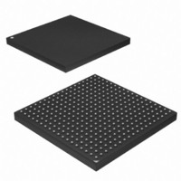
IC MCU ARM9 APMC 324TFBGA
Manufacturer
Atmel
Series
AT91SAMr
Datasheet
1.AT91SAM9G45-EKES.pdf
(1218 pages)
Specifications of AT91SAM9G45-CU-999
Core Processor
ARM9
Core Size
16/32-Bit
Speed
400MHz
Connectivity
EBI/EMI, Ethernet, I²C, IrDA, MMC, SPI, SSC, UART/USART, USB
Peripherals
AC'97, DMA, I²S, LCD, POR, PWM, WDT
Number Of I /o
160
Program Memory Size
64KB (64K x 8)
Program Memory Type
ROM
Ram Size
128K x 8
Voltage - Supply (vcc/vdd)
0.9 V ~ 1.1 V
Data Converters
A/D 8x10b
Oscillator Type
Internal
Operating Temperature
-40°C ~ 85°C
Package / Case
324-TFBGA
Lead Free Status / RoHS Status
Lead free / RoHS Compliant
Eeprom Size
-
Lead Free Status / Rohs Status
Supplier Unconfirmed
Available stocks
Company
Part Number
Manufacturer
Quantity
Price


234
AT91SAM9G45
An additional 200 cycles of clock are required for locking DLL
8. An Extended Mode Register set (EMRS1) cycle is issued to enable DLL. The applica-
9. Program DLL field into the Configuration Register (see
10. A Mode Register set (MRS) cycle is issued to reset DLL. The application must set
11. An all banks precharge command is issued to the DDR2-SDRAM. Program all banks
12. Two auto-refresh (CBR) cycles are provided. Program the auto refresh command
13. Program DLL field into the Configuration Register (see
14. A Mode Register set (MRS) cycle is issued to program the parameters of the DDR2-
15. Program OCD field into the Configuration Register (see
16. An Extended Mode Register set (EMRS1) cycle is issued to OCD default value. The
17. Program OCD field into the Configuration Register (see
18. An Extended Mode Register set (EMRS1) cycle is issued to enable OCD exit. The
tion must set Mode to 5 in the Mode Register (see
perform a write access to the DDR2-SDRAM to acknowledge this command. The write
address must be chosen so that BA[1] is set to 0 and BA[0] is set to 1. For example,
with a 16-bit 128 MB DDR2-SDRAM (12 rows, 9 columns, 4 banks) bank address, the
DDR2-SDRAM write access should be done at the address 0x20400000.
high (Enable DLL reset).
Mode to 3 in the Mode Register (see
access to the DDR2-SDRAM to acknowledge this command. The write address must
be chosen so that BA[1:0] bits are set to 0. For example, with a 16-bit 128 MB DDR2-
SDRAM (12 rows, 9 columns, 4 banks) bank address, the SDRAM write access should
be done at the address 0x20000000.
precharge command into the Mode Register, the application must set Mode to 2 in the
Mode Register (See
SDRAM address to acknowledge this command
(CBR) into the Mode Register, the application must set Mode to 4 in the Mode Register
(see
tion twice to acknowledge these commands.
low (Disable DLL reset).
SDRAM devices, in particular CAS latency, burst length and to disable DLL reset. The
application must set Mode to 3 in the Mode Register (see
and perform a write access to the DDR2-SDRAM to acknowledge this command. The
write address must be chosen so that BA[1:0] are set to 0. For example, with a 16-bit
128 MB SDRAM (12 rows, 9 columns, 4 banks) bank address, the SDRAM write
access should be done at the address 0x20000000
high (OCD calibration default).
application must set Mode to 5 in the Mode Register (see
and perform a write access to the DDR2-SDRAM to acknowledge this command. The
write address must be chosen so that BA[1] is set to 0 and BA[0] is set to 1. For exam-
ple, with a 16-bit 128 MB DDR2-SDRAM (12 rows, 9 columns, 4 banks) bank address,
the DDR2-SDRAM write access should be done at the address 0x20400000.
low (OCD calibration mode exit).
application must set Mode to 5 in the Mode Register (see
and perform a write access to the DDR2-SDRAM to acknowledge this command. The
write address must be chosen so that BA[1] is set to 0 and BA[0] is set to 1. For exam-
ple, with a 16-bit 128 MB DDR2-SDRAM (12 rows, 9 columns, 4 banks) bank address,
the DDR2-SDRAM write access should be done at the address 0x20400000.
Section 22.7.1 on page
Section 22.7.1 on page
260). Performs a write access to any DDR2-SDRAM loca-
Section 22.7.1 on page
260). Perform a write access to any DDR2-
Section 22.7.1 on page
Section 22.7.3 on page
Section 22.7.3 on page
Section 22.7.3 on page
Section 22.7.3 on page
Section 22.7.1 on page
Section 22.7.1 on page
Section 22.7.1 on page
260) and perform a write
6438F–ATARM–21-Jun-10
260) and
262) to
262) to
262) to
262) to
260)
260)
260)
Related parts for AT91SAM9G45-CU-999
Image
Part Number
Description
Manufacturer
Datasheet
Request
R

Part Number:
Description:
KIT EVAL FOR AT91SAM9G45
Manufacturer:
Atmel
Datasheet:

Part Number:
Description:
MCU ARM9 324-TFBGA
Manufacturer:
Atmel
Datasheet:

Part Number:
Description:
At91 Arm Thumb-based Microcontrollers
Manufacturer:
ATMEL Corporation
Datasheet:

Part Number:
Description:
MCU, MPU & DSP Development Tools KICKSTART KIT FOR AT91SAM9 PLUS
Manufacturer:
IAR Systems

Part Number:
Description:
DEV KIT FOR AVR/AVR32
Manufacturer:
Atmel
Datasheet:
Part Number:
Description:
INTERVAL AND WIPE/WASH WIPER CONTROL IC WITH DELAY
Manufacturer:
ATMEL Corporation
Datasheet:
Part Number:
Description:
Low-Voltage Voice-Switched IC for Hands-Free Operation
Manufacturer:
ATMEL Corporation
Datasheet:
Part Number:
Description:
MONOLITHIC INTEGRATED FEATUREPHONE CIRCUIT
Manufacturer:
ATMEL Corporation
Datasheet:
Part Number:
Description:
AM-FM Receiver IC U4255BM-M
Manufacturer:
ATMEL Corporation
Datasheet:
Part Number:
Description:
Monolithic Integrated Feature Phone Circuit
Manufacturer:
ATMEL Corporation
Datasheet:
Part Number:
Description:
Multistandard Video-IF and Quasi Parallel Sound Processing
Manufacturer:
ATMEL Corporation
Datasheet:
Part Number:
Description:
High-performance EE PLD
Manufacturer:
ATMEL Corporation
Datasheet: