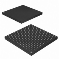
AT91SAM9G45-CU-999 Atmel, AT91SAM9G45-CU-999 Datasheet - Page 683

AT91SAM9G45-CU-999
Manufacturer Part Number
AT91SAM9G45-CU-999
Description
IC MCU ARM9 APMC 324TFBGA
Manufacturer
Atmel
Series
AT91SAMr
Datasheet
1.AT91SAM9G45-EKES.pdf
(1218 pages)
Specifications of AT91SAM9G45-CU-999
Core Processor
ARM9
Core Size
16/32-Bit
Speed
400MHz
Connectivity
EBI/EMI, Ethernet, I²C, IrDA, MMC, SPI, SSC, UART/USART, USB
Peripherals
AC'97, DMA, I²S, LCD, POR, PWM, WDT
Number Of I /o
160
Program Memory Size
64KB (64K x 8)
Program Memory Type
ROM
Ram Size
128K x 8
Voltage - Supply (vcc/vdd)
0.9 V ~ 1.1 V
Data Converters
A/D 8x10b
Oscillator Type
Internal
Operating Temperature
-40°C ~ 85°C
Package / Case
324-TFBGA
Lead Free Status / RoHS Status
Lead free / RoHS Compliant
Eeprom Size
-
Lead Free Status / Rohs Status
Supplier Unconfirmed
Available stocks
Company
Part Number
Manufacturer
Quantity
Price
- Current page: 683 of 1218
- Download datasheet (19Mb)
34.9.3
Name:
Addresses:
Access:
• CKS: Receive Clock Selection
• CKO: Receive Clock Output Mode Selection
• CKI: Receive Clock Inversion
0 = The data inputs (Data and Frame Sync signals) are sampled on Receive Clock falling edge. The Frame Sync signal
output is shifted out on Receive Clock rising edge.
1 = The data inputs (Data and Frame Sync signals) are sampled on Receive Clock rising edge. The Frame Sync signal out-
put is shifted out on Receive Clock falling edge.
CKI affects only the Receive Clock and not the output clock signal.
6438F–ATARM–21-Jun-10
0x3-0x7
31
23
15
–
7
CKO
CKS
0x0
0x1
0x2
0x0
0x1
0x2
0x3
SSC Receive Clock Mode Register
CKG
Receive Clock Output Mode
None
Continuous Receive Clock
Receive Clock only during data transfers
Reserved
Selected Receive Clock
Divided Clock
TK Clock signal
RK pin
Reserved
30
22
14
SSC_RCMR
0xFFF9C010 (0), 0xFFFA0010 (1)
Read-write
–
6
CKI
29
21
13
–
5
STOP
28
20
12
4
PERIOD
STTDLY
CKO
27
19
11
3
26
18
10
2
START
AT91SAM9G45
25
17
9
1
Input-only
CKS
RK pin
Output
Output
24
16
8
0
683
Related parts for AT91SAM9G45-CU-999
Image
Part Number
Description
Manufacturer
Datasheet
Request
R

Part Number:
Description:
KIT EVAL FOR AT91SAM9G45
Manufacturer:
Atmel
Datasheet:

Part Number:
Description:
MCU ARM9 324-TFBGA
Manufacturer:
Atmel
Datasheet:

Part Number:
Description:
At91 Arm Thumb-based Microcontrollers
Manufacturer:
ATMEL Corporation
Datasheet:

Part Number:
Description:
MCU, MPU & DSP Development Tools KICKSTART KIT FOR AT91SAM9 PLUS
Manufacturer:
IAR Systems

Part Number:
Description:
DEV KIT FOR AVR/AVR32
Manufacturer:
Atmel
Datasheet:

Part Number:
Description:
INTERVAL AND WIPE/WASH WIPER CONTROL IC WITH DELAY
Manufacturer:
ATMEL Corporation
Datasheet:

Part Number:
Description:
Low-Voltage Voice-Switched IC for Hands-Free Operation
Manufacturer:
ATMEL Corporation
Datasheet:

Part Number:
Description:
MONOLITHIC INTEGRATED FEATUREPHONE CIRCUIT
Manufacturer:
ATMEL Corporation
Datasheet:

Part Number:
Description:
AM-FM Receiver IC U4255BM-M
Manufacturer:
ATMEL Corporation
Datasheet:

Part Number:
Description:
Monolithic Integrated Feature Phone Circuit
Manufacturer:
ATMEL Corporation
Datasheet:

Part Number:
Description:
Multistandard Video-IF and Quasi Parallel Sound Processing
Manufacturer:
ATMEL Corporation
Datasheet:

Part Number:
Description:
High-performance EE PLD
Manufacturer:
ATMEL Corporation
Datasheet:


