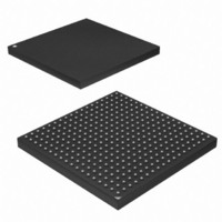
AT91SAM9G45-CU-999 Atmel, AT91SAM9G45-CU-999 Datasheet - Page 897

AT91SAM9G45-CU-999
Manufacturer Part Number
AT91SAM9G45-CU-999
Description
IC MCU ARM9 APMC 324TFBGA
Manufacturer
Atmel
Series
AT91SAMr
Datasheet
1.AT91SAM9G45-EKES.pdf
(1218 pages)
Specifications of AT91SAM9G45-CU-999
Core Processor
ARM9
Core Size
16/32-Bit
Speed
400MHz
Connectivity
EBI/EMI, Ethernet, I²C, IrDA, MMC, SPI, SSC, UART/USART, USB
Peripherals
AC'97, DMA, I²S, LCD, POR, PWM, WDT
Number Of I /o
160
Program Memory Size
64KB (64K x 8)
Program Memory Type
ROM
Ram Size
128K x 8
Voltage - Supply (vcc/vdd)
0.9 V ~ 1.1 V
Data Converters
A/D 8x10b
Oscillator Type
Internal
Operating Temperature
-40°C ~ 85°C
Package / Case
324-TFBGA
Lead Free Status / RoHS Status
Lead free / RoHS Compliant
Eeprom Size
-
Lead Free Status / Rohs Status
Supplier Unconfirmed
Available stocks
Company
Part Number
Manufacturer
Quantity
Price
- Current page: 897 of 1218
- Download datasheet (19Mb)
39.4
39.4.1
6438F–ATARM–21-Jun-10
Functional Description
Data Timing
The Image Sensor Interface (ISI) supports direct connection to the ITU-R BT. 601/656 8-bit
mode compliant sensors and up to 12-bit grayscale sensors. It receives the image data stream
from the image sensor on the 12-bit data bus.
This module receives up to 12 bits for data, the horizontal and vertical synchronizations and the
pixel clock. The reduced pin count alternative for synchronization is supported for sensors that
embed SAV (start of active video) and EAV (end of active video) delimiters in the data stream.
The Image Sensor Interface interrupt line is connected to the Advanced Interrupt Controller and
can trigger an interrupt at the beginning of each frame and at the end of a DMA frame transfer. If
the SAV/EAV synchronization is used, an interrupt can be triggered on each delimiter event.
For 8-bit color sensors, the data stream received can be in several possible formats: YCbCr
4:2:2, RGB 8:8:8, RGB 5:6:5 and may be processed before the storage in memory. The data
stream may be sent on both preview path and codec path if the bit ISI_CDC in the ISI_CTRL is
one. To optimize the bandwidth, the codec path should be enabled only when a capture is
required.
In grayscale mode, the input data stream is stored in memory without any processing. The 12-bit
data, which represent the grayscale level for the pixel, is stored in memory one or two pixels per
word, depending on the GS_MODE bit in the ISI_CFG2 register. The codec datapath is not
available when grayscale image is selected.
A frame rate counter allows users to capture all frames or 1 out of every 2 to 8 frames.
The two data timings using horizontal and vertical synchronization and EAV/SAV sequence syn-
chronization are shown in
In the VSYNC/HSYNC synchronization, the valid data is captured with the active edge of the
pixel clock (ISI_PCK), after SFD lines of vertical blanking and SLD pixel clock periods delay pro-
grammed in the control register.
The ITU-RBT.656-4 defines the functional timing for an 8-bit wide interface.
There are two timing reference signals, one at the beginning of each video data block SAV
(0xFF000080) and one at the end of each video data block EAV(0xFF00009D). Only data sent
between EAV and SAV is captured. Horizontal blanking and vertical blanking are ignored. Use of
the SAV and EAV synchronization eliminates the ISI_VSYNC and ISI_HSYNC signals from the
interface, thereby reducing the pin count. In order to retrieve both frame and line synchronization
properly, at least one line of vertical blanking is mandatory.
Figure 39-3
and
Figure
39-4.
AT91SAM9G45
897
Related parts for AT91SAM9G45-CU-999
Image
Part Number
Description
Manufacturer
Datasheet
Request
R

Part Number:
Description:
KIT EVAL FOR AT91SAM9G45
Manufacturer:
Atmel
Datasheet:

Part Number:
Description:
MCU ARM9 324-TFBGA
Manufacturer:
Atmel
Datasheet:

Part Number:
Description:
At91 Arm Thumb-based Microcontrollers
Manufacturer:
ATMEL Corporation
Datasheet:

Part Number:
Description:
MCU, MPU & DSP Development Tools KICKSTART KIT FOR AT91SAM9 PLUS
Manufacturer:
IAR Systems

Part Number:
Description:
DEV KIT FOR AVR/AVR32
Manufacturer:
Atmel
Datasheet:

Part Number:
Description:
INTERVAL AND WIPE/WASH WIPER CONTROL IC WITH DELAY
Manufacturer:
ATMEL Corporation
Datasheet:

Part Number:
Description:
Low-Voltage Voice-Switched IC for Hands-Free Operation
Manufacturer:
ATMEL Corporation
Datasheet:

Part Number:
Description:
MONOLITHIC INTEGRATED FEATUREPHONE CIRCUIT
Manufacturer:
ATMEL Corporation
Datasheet:

Part Number:
Description:
AM-FM Receiver IC U4255BM-M
Manufacturer:
ATMEL Corporation
Datasheet:

Part Number:
Description:
Monolithic Integrated Feature Phone Circuit
Manufacturer:
ATMEL Corporation
Datasheet:

Part Number:
Description:
Multistandard Video-IF and Quasi Parallel Sound Processing
Manufacturer:
ATMEL Corporation
Datasheet:

Part Number:
Description:
High-performance EE PLD
Manufacturer:
ATMEL Corporation
Datasheet:


