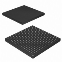
AT91SAM9G45-CU-999 Atmel, AT91SAM9G45-CU-999 Datasheet - Page 1113

AT91SAM9G45-CU-999
Manufacturer Part Number
AT91SAM9G45-CU-999
Description
IC MCU ARM9 APMC 324TFBGA
Manufacturer
Atmel
Series
AT91SAMr
Datasheet
1.AT91SAM9G45-EKES.pdf
(1218 pages)
Specifications of AT91SAM9G45-CU-999
Core Processor
ARM9
Core Size
16/32-Bit
Speed
400MHz
Connectivity
EBI/EMI, Ethernet, I²C, IrDA, MMC, SPI, SSC, UART/USART, USB
Peripherals
AC'97, DMA, I²S, LCD, POR, PWM, WDT
Number Of I /o
160
Program Memory Size
64KB (64K x 8)
Program Memory Type
ROM
Ram Size
128K x 8
Voltage - Supply (vcc/vdd)
0.9 V ~ 1.1 V
Data Converters
A/D 8x10b
Oscillator Type
Internal
Operating Temperature
-40°C ~ 85°C
Package / Case
324-TFBGA
Lead Free Status / RoHS Status
Lead free / RoHS Compliant
Eeprom Size
-
Lead Free Status / Rohs Status
Supplier Unconfirmed
Available stocks
Company
Part Number
Manufacturer
Quantity
Price
- Current page: 1113 of 1218
- Download datasheet (19Mb)
45.6.2.10
45.6.2.11
6438F–ATARM–21-Jun-10
Display
PWM
HFP
=
f
LCDDOTCK
In monochrome mode, Horizontal_display_size is equal to the number of horizontal pixels. The
number_data_lines is equal to the number of bits of the interface in single scan mode;
number_data_lines is equal to half the bits of the interface in dual scan mode.
In color mode, Horizontal_display_size equals three times the number of horizontal pixels.
In TFT Mode:
The frame rate equation is used first without considering the clock periods added at the end
beginning or at the end of each line to determine, approximately, the LCDDOTCK rate:
With this value, the CLKVAL is fixed, as well as the corresponding LCDDOTCK rate.
Then select VHDLY, HPW and HBP according to the type of LCD used and
page
Finally, the frame rate is adjusted to 70 Hz - 75 Hz with the HFP value:
The line counting is controlled by the read-only field LINECNT of LCDCON1 register. The LINE-
CNT field decreases by one unit at each falling edge of LCDHSYNC.
This block is used to configure the polarity of the data and control signals. The polarity of all
clock signals can be configured by LCDCON2[12:8] register setting.
This block also generates the lcd_pwr signal internally used to control the state of the LCD pins
and to turn on and off by software the LCD module.
It is also available on the LCDPWR pin.
This signal is controlled by the PWRCON register and respects the number of frames configured
in the GUARD_TIME field of PWRCON register (PWRCON[7:1]) between the write access to
LCD_PWR field (PWRCON[0]) and the activation/deactivation of lcd_pwr signal.
The minimum value for the GUARD_TIME field is one frame. This gives the DMA Controller
enough time to fill the FIFOs before the start of data transfer to the LCD.
This block generates the LCD contrast control signal (LCDCC) to make possible the control of
the display's contrast by software. This is an 8-bit PWM (Pulse Width Modulation) signal that can
be converted to an analog voltage with a simple passive filter.
1110.
------------------------------------------------------------------------------------------------------------- -
f
LCDVSYNC
LINEVAL
HOZVAL
LINEVAL
f
lcd_pclk
=
LINEVAL
=
=
=
HOZVAL
Horizontal_display_size 1
Vertical_display_size 1
Vertical_display_size 1
1
+
VBP
+
5
+
VFP
f
lcd_vsync
+
–
–
1
–
–
LINEVAL
VHDLY
+
+
HPW
1
AT91SAM9G45
+
HPB
+
“Equation 1” on
HOZVAL
+
1113
4
Related parts for AT91SAM9G45-CU-999
Image
Part Number
Description
Manufacturer
Datasheet
Request
R

Part Number:
Description:
KIT EVAL FOR AT91SAM9G45
Manufacturer:
Atmel
Datasheet:

Part Number:
Description:
MCU ARM9 324-TFBGA
Manufacturer:
Atmel
Datasheet:

Part Number:
Description:
At91 Arm Thumb-based Microcontrollers
Manufacturer:
ATMEL Corporation
Datasheet:

Part Number:
Description:
MCU, MPU & DSP Development Tools KICKSTART KIT FOR AT91SAM9 PLUS
Manufacturer:
IAR Systems

Part Number:
Description:
DEV KIT FOR AVR/AVR32
Manufacturer:
Atmel
Datasheet:

Part Number:
Description:
INTERVAL AND WIPE/WASH WIPER CONTROL IC WITH DELAY
Manufacturer:
ATMEL Corporation
Datasheet:

Part Number:
Description:
Low-Voltage Voice-Switched IC for Hands-Free Operation
Manufacturer:
ATMEL Corporation
Datasheet:

Part Number:
Description:
MONOLITHIC INTEGRATED FEATUREPHONE CIRCUIT
Manufacturer:
ATMEL Corporation
Datasheet:

Part Number:
Description:
AM-FM Receiver IC U4255BM-M
Manufacturer:
ATMEL Corporation
Datasheet:

Part Number:
Description:
Monolithic Integrated Feature Phone Circuit
Manufacturer:
ATMEL Corporation
Datasheet:

Part Number:
Description:
Multistandard Video-IF and Quasi Parallel Sound Processing
Manufacturer:
ATMEL Corporation
Datasheet:

Part Number:
Description:
High-performance EE PLD
Manufacturer:
ATMEL Corporation
Datasheet:


