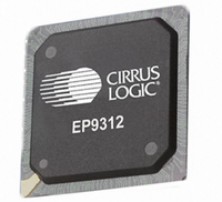
EP9312-CBZ Cirrus Logic Inc, EP9312-CBZ Datasheet - Page 142

EP9312-CBZ
Manufacturer Part Number
EP9312-CBZ
Description
IC ARM9 SOC UNIVERSAL 352PBGA
Manufacturer
Cirrus Logic Inc
Series
EP9r
Specifications of EP9312-CBZ
Core Size
16/32-Bit
Core Processor
ARM9
Speed
200MHz
Connectivity
EBI/EMI, EIDE, Ethernet, I²C, IrDA, Keypad/Touchscreen, SPI, UART/USART, USB
Peripherals
AC'97, DMA, I²:S, LCD, LED, MaverickKey, POR, PWM, WDT
Number Of I /o
16
Program Memory Type
ROMless
Ram Size
32K x 8
Voltage - Supply (vcc/vdd)
1.65 V ~ 3.6 V
Data Converters
A/D 8x12b
Oscillator Type
External
Operating Temperature
0°C ~ 70°C
Package / Case
352-BGA
Controller Family/series
(ARM9)
No. Of I/o's
16
Ram Memory Size
16MB
Cpu Speed
200MHz
No. Of Timers
4
No. Of Pwm Channels
2
Digital Ic Case Style
BGA
Embedded Interface Type
AC97, I2S, SPI, UART, USB
Rohs Compliant
Yes
Processor Series
EP93xx
Core
ARM920T
Data Bus Width
32 bit
3rd Party Development Tools
MDK-ARM, RL-ARM, ULINK2
Lead Free Status / RoHS Status
Lead free / RoHS Compliant
Eeprom Size
-
Program Memory Size
-
Lead Free Status / Rohs Status
Details
Other names
598-1258
Available stocks
Company
Part Number
Manufacturer
Quantity
Price
- Current page: 142 of 824
- Download datasheet (13Mb)
5
5-16
System Controller
EP93xx User’s Guide
DMA M2M/P CHx: These bits enable the clocks to the DMA controller
USH_EN:
UARTBAUD:
FIR_EN:
Copyright 2007 Cirrus Logic
channels. Note that a channels-enable bit MUST be
asserted before any register within the DMA controller can
be read or written. At least one ARM instruction cycle must
occur between writing to this register to enable the DMA
Controller channel and actually accessing it. The number
of cycles will depend on the setting of HCLK and PCLK
division in the
power, ensure that all these bits are disabled (low) if the
DMA controller is not being used. On a system reset, the
register will be reset to zero.
This bit is used to gate the HCLK to the USB Host block in
order to save power. It is reset to zero, thus gating off the
HCLK. It can be set to one to turn on the HCLK to the USB
Host. This bit must be set before any register within the
USB Host can be accessed. At least one ARM instruction
cycle must occur between writing to this register bit and
actually accessing the USB Host. The number of cycles
will depend on the setting of HCLK and PCLK division in
the
This bit is also used to gate the 48 MHz and 12 MHz
clocks to the USB Host block in order to save power. It is
reset to zero, thus gating off the USB Host clocks. By
setting this to one, the USB Host clocks are enabled. At
least one ARM instruction cycle must occur between
writing to this register bit and actually accessing the USB
Host. The number of cycles will depend on the wake-up
time for PLL2. To find out if PLL2 has locked on to its
frequency, the PLL2_LOCK bit in the PwrSts register can
be read.
This bit controls the clock input to the UARTs. When
cleared, the UARTs are driven by the 14.7456 MHz clock
divided by 2 (7.3728 MHz). This gives a maximum baud-
rate of 230 Kbps. When set, the UARTs are driven by the
14.7456 MHz clock directly, giving an increased maximum
baud rate of 460 Kbps. This bit is 0 on reset.
This bit is used to gate the FIRCLK to the IrDA block in
order to save power. It is reset to zero, thus gating off the
FIRCLK. Setting this bit to one will turn on the 48 MHz
clock to the IrDA.
"ClkSet1"
and
"ClkSet1"
"ClkSet2"
or
register.s
"ClkSet2"
register. To save
DS785UM1
Related parts for EP9312-CBZ
Image
Part Number
Description
Manufacturer
Datasheet
Request
R

Part Number:
Description:
IC ARM920T MCU 200MHZ 352-PBGA
Manufacturer:
Cirrus Logic Inc
Datasheet:

Part Number:
Description:
System-on-Chip Processor
Manufacturer:
Cirrus Logic Inc
Datasheet:

Part Number:
Description:
IC ARM920T MCU 200MHZ 352-PBGA
Manufacturer:
Cirrus Logic Inc
Datasheet:

Part Number:
Description:
Development Kit
Manufacturer:
Cirrus Logic Inc
Datasheet:

Part Number:
Description:
Development Kit
Manufacturer:
Cirrus Logic Inc
Datasheet:

Part Number:
Description:
High-efficiency PFC + Fluorescent Lamp Driver Reference Design
Manufacturer:
Cirrus Logic Inc
Datasheet:

Part Number:
Description:
Development Kit
Manufacturer:
Cirrus Logic Inc
Datasheet:

Part Number:
Description:
Development Kit
Manufacturer:
Cirrus Logic Inc
Datasheet:

Part Number:
Description:
Development Kit
Manufacturer:
Cirrus Logic Inc
Datasheet:

Part Number:
Description:
Development Kit
Manufacturer:
Cirrus Logic Inc
Datasheet:

Part Number:
Description:
Development Kit
Manufacturer:
Cirrus Logic Inc
Datasheet:

Part Number:
Description:
Development Kit
Manufacturer:
Cirrus Logic Inc
Datasheet:

Part Number:
Description:
Ref Bd For Speakerbar MSA & DSP Products
Manufacturer:
Cirrus Logic Inc


