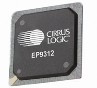
EP9312-CBZ Cirrus Logic Inc, EP9312-CBZ Datasheet - Page 506

EP9312-CBZ
Manufacturer Part Number
EP9312-CBZ
Description
IC ARM9 SOC UNIVERSAL 352PBGA
Manufacturer
Cirrus Logic Inc
Series
EP9r
Specifications of EP9312-CBZ
Core Size
16/32-Bit
Core Processor
ARM9
Speed
200MHz
Connectivity
EBI/EMI, EIDE, Ethernet, I²C, IrDA, Keypad/Touchscreen, SPI, UART/USART, USB
Peripherals
AC'97, DMA, I²:S, LCD, LED, MaverickKey, POR, PWM, WDT
Number Of I /o
16
Program Memory Type
ROMless
Ram Size
32K x 8
Voltage - Supply (vcc/vdd)
1.65 V ~ 3.6 V
Data Converters
A/D 8x12b
Oscillator Type
External
Operating Temperature
0°C ~ 70°C
Package / Case
352-BGA
Controller Family/series
(ARM9)
No. Of I/o's
16
Ram Memory Size
16MB
Cpu Speed
200MHz
No. Of Timers
4
No. Of Pwm Channels
2
Digital Ic Case Style
BGA
Embedded Interface Type
AC97, I2S, SPI, UART, USB
Rohs Compliant
Yes
Processor Series
EP93xx
Core
ARM920T
Data Bus Width
32 bit
3rd Party Development Tools
MDK-ARM, RL-ARM, ULINK2
Lead Free Status / RoHS Status
Lead free / RoHS Compliant
Eeprom Size
-
Program Memory Size
-
Lead Free Status / Rohs Status
Details
Other names
598-1258
Available stocks
Company
Part Number
Manufacturer
Quantity
Price
- Current page: 506 of 824
- Download datasheet (13Mb)
13
13-10
SDRAM, SyncROM, and SyncFLASH Controller
EP93xx User’s Guide
13.8.2 Address/Data/Control Required by Memory System
An independent device configuration register, "SDRAMDevCfg[3:0]", "SDRAMDevCfg[3:0]",
"SDRAMDevCfg[3:0]", and "SDRAMDevCfg[3:0]", is provided for each of the four
synchronous memory domains. Each domain can be configured for either an SDRAM,
SyncROM, or SyncFLASH device type. Only one device type can be configured per domain.
However, different domains can be configured for different device types.
Each of the four synchronous memory domains can be configured to be either 16- or 32-bits
wide and each will support 32-bit (word), 16-bit (half-word), and 8-bit (byte) accesses to or
from the synchronous memory device. If the external memory bus is 16-bits wide, two
external bus accesses are automatically made to Read or Write a 32-bit word. This is why a
burst-of-eight accesses is used to Read or Write devices that are attached to a 16-bit bus
while only a burst-of-four accesses is used to Read or Write devices that are attached to a
32-bit bus.
When writing to external memory, byte lane enable signals are output on the nDQM[3:0] pins,
where the DQMn0 pin controls the least-significant byte lane, the DQMn1 pin controls the
next to least-significant byte lane, the DQMn2 pin controls the next to most- significant byte
lane, and the DQMn3 pin controls the most-significant byte lane. The memory device uses
the byte lane enable signals on the DQMn pins to determine which byte lane data it should
accept during a Write operation. For example, if a 32-bit word is to be written to a memory
device on a 32-bit memory bus, DQMn[3:0] = ‘0000’ is output to alert the memory device that
it should accept Write data from all four byte lanes. However, if an 8-bit byte is to be written to
the next to least-significant byte of a memory device on a 32-bit bus, DQMn[3:0] = ‘1101’ is
output to alert the memory device that it should accept Write data from only the next to least-
significant byte lane and reject Write data from the other byte lanes. As another example, if a
32-bit word is to be written to a memory device on a 16-bit data bus, two 16-bit writes are
automatically performed to the memory device. For each 16-bit Write, DQM[1:0] = ‘00’ and
DQM[3:2] are not used.
device with 13-row x 9-column x 2-bank addressing attached to a 16-bit memory bus. Note
Table 13-10
Boot Option
(ASDO)
X
X
X
0
shows a memory addressing example for a 256 Mbit synchronous memory
A31
1
1
1
1
Table 13-9. Chip Select Decoding
Copyright 2007 Cirrus Logic
A30
1
1
1
1
A29
1
1
0
0
A28
1
0
1
0
Chip select
nSDCS3
nSDCS2
nSDCS1
nSDCS0
DS785UM1
Related parts for EP9312-CBZ
Image
Part Number
Description
Manufacturer
Datasheet
Request
R

Part Number:
Description:
IC ARM920T MCU 200MHZ 352-PBGA
Manufacturer:
Cirrus Logic Inc
Datasheet:

Part Number:
Description:
System-on-Chip Processor
Manufacturer:
Cirrus Logic Inc
Datasheet:

Part Number:
Description:
IC ARM920T MCU 200MHZ 352-PBGA
Manufacturer:
Cirrus Logic Inc
Datasheet:

Part Number:
Description:
Development Kit
Manufacturer:
Cirrus Logic Inc
Datasheet:

Part Number:
Description:
Development Kit
Manufacturer:
Cirrus Logic Inc
Datasheet:

Part Number:
Description:
High-efficiency PFC + Fluorescent Lamp Driver Reference Design
Manufacturer:
Cirrus Logic Inc
Datasheet:

Part Number:
Description:
Development Kit
Manufacturer:
Cirrus Logic Inc
Datasheet:

Part Number:
Description:
Development Kit
Manufacturer:
Cirrus Logic Inc
Datasheet:

Part Number:
Description:
Development Kit
Manufacturer:
Cirrus Logic Inc
Datasheet:

Part Number:
Description:
Development Kit
Manufacturer:
Cirrus Logic Inc
Datasheet:

Part Number:
Description:
Development Kit
Manufacturer:
Cirrus Logic Inc
Datasheet:

Part Number:
Description:
Development Kit
Manufacturer:
Cirrus Logic Inc
Datasheet:

Part Number:
Description:
Ref Bd For Speakerbar MSA & DSP Products
Manufacturer:
Cirrus Logic Inc


