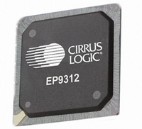
EP9312-CBZ Cirrus Logic Inc, EP9312-CBZ Datasheet - Page 773

EP9312-CBZ
Manufacturer Part Number
EP9312-CBZ
Description
IC ARM9 SOC UNIVERSAL 352PBGA
Manufacturer
Cirrus Logic Inc
Series
EP9r
Specifications of EP9312-CBZ
Core Size
16/32-Bit
Core Processor
ARM9
Speed
200MHz
Connectivity
EBI/EMI, EIDE, Ethernet, I²C, IrDA, Keypad/Touchscreen, SPI, UART/USART, USB
Peripherals
AC'97, DMA, I²:S, LCD, LED, MaverickKey, POR, PWM, WDT
Number Of I /o
16
Program Memory Type
ROMless
Ram Size
32K x 8
Voltage - Supply (vcc/vdd)
1.65 V ~ 3.6 V
Data Converters
A/D 8x12b
Oscillator Type
External
Operating Temperature
0°C ~ 70°C
Package / Case
352-BGA
Controller Family/series
(ARM9)
No. Of I/o's
16
Ram Memory Size
16MB
Cpu Speed
200MHz
No. Of Timers
4
No. Of Pwm Channels
2
Digital Ic Case Style
BGA
Embedded Interface Type
AC97, I2S, SPI, UART, USB
Rohs Compliant
Yes
Processor Series
EP93xx
Core
ARM920T
Data Bus Width
32 bit
3rd Party Development Tools
MDK-ARM, RL-ARM, ULINK2
Lead Free Status / RoHS Status
Lead free / RoHS Compliant
Eeprom Size
-
Program Memory Size
-
Lead Free Status / Rohs Status
Details
Other names
598-1258
Available stocks
Company
Part Number
Manufacturer
Quantity
Price
- Current page: 773 of 824
- Download datasheet (13Mb)
DS785UM1
27.2.2 PIO Operations
For PIO operations, the Pin Interface unit handles all the operations. Register read and write
operations by the host are sufficient to operate the IDE interface in PIO mode for both non-
data and data transfer in both directions.
Most IDE controllers handle this automatically, but this IDE controller does not. The diagrams
are located in Information Technology AT Attachment with Packet Interface (ATA/ATAPI-5),
Section 10.2.2, Figure 44. See
additional information.
Initial state: pins DIORn and DIOWn low.
For a Read operation.
Note: NI = Not supported at this time.
1. Write out the register value.
2. Delay as follows, based on the PIO mode.
3. Bring DIORn high.
4. Based on the PIO mode, delay as follows before the next read or write can occur.
5. Bring DIORn low.
6. Read IDE Data in the register.
PIO Mode 0 - Delay for 70 ns
PIO Mode 1 - Delay for 50 ns.
PIO Mode 2 - Delay for 30 ns.
PIO Mode 3 - Delay for 30 ns
PIO Mode 4 - Delay for 25 ns
PIO Mode 0 - Delay for 290 ns.
PIO Mode 1 - Delay for 290 ns
PIO Mode 2 - Delay for 290 ns.
PIO Mode 3 - Delay for 80 ns
PIO Mode 4 - Delay for 70 ns
DDMARDYn/
DSTROBE
IOCS16n
IDE Pin
PDIAGn/
DD[15:0]
IORDY/
CBLIDn
Table 27-1. IDE Host to IDE Interface Definition (Continued)
Type
NI
NI
-
-
Copyright 2007 Cirrus Logic
No. of
"Preface"
Pins
16
1
1
1
Negate to extend the host transfer cycle of any host read or
write access/
Flow control signal for Ultra DMA data-out burst/
Flow control signal for Ultra DMA data-in burst
Device indicates it supports 16-bit I/O bus cycles
Asserted by device 1 to indicate to device 0 that it has finished
diagnostic/
Cable assembly type identifier
16-bit data interface between controller and device
chapter,
“Reference Documents” on page P-3
Description
EP93xx User’s Guide
IDE Interface
for
27-3
27
Related parts for EP9312-CBZ
Image
Part Number
Description
Manufacturer
Datasheet
Request
R

Part Number:
Description:
IC ARM920T MCU 200MHZ 352-PBGA
Manufacturer:
Cirrus Logic Inc
Datasheet:

Part Number:
Description:
System-on-Chip Processor
Manufacturer:
Cirrus Logic Inc
Datasheet:

Part Number:
Description:
IC ARM920T MCU 200MHZ 352-PBGA
Manufacturer:
Cirrus Logic Inc
Datasheet:

Part Number:
Description:
Development Kit
Manufacturer:
Cirrus Logic Inc
Datasheet:

Part Number:
Description:
Development Kit
Manufacturer:
Cirrus Logic Inc
Datasheet:

Part Number:
Description:
High-efficiency PFC + Fluorescent Lamp Driver Reference Design
Manufacturer:
Cirrus Logic Inc
Datasheet:

Part Number:
Description:
Development Kit
Manufacturer:
Cirrus Logic Inc
Datasheet:

Part Number:
Description:
Development Kit
Manufacturer:
Cirrus Logic Inc
Datasheet:

Part Number:
Description:
Development Kit
Manufacturer:
Cirrus Logic Inc
Datasheet:

Part Number:
Description:
Development Kit
Manufacturer:
Cirrus Logic Inc
Datasheet:

Part Number:
Description:
Development Kit
Manufacturer:
Cirrus Logic Inc
Datasheet:

Part Number:
Description:
Development Kit
Manufacturer:
Cirrus Logic Inc
Datasheet:

Part Number:
Description:
Ref Bd For Speakerbar MSA & DSP Products
Manufacturer:
Cirrus Logic Inc


