DF36912GFH Renesas Electronics America, DF36912GFH Datasheet - Page 23
DF36912GFH
Manufacturer Part Number
DF36912GFH
Description
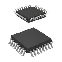
MCU 3/5V 8K 32-LQFP
Manufacturer
Renesas Electronics America
Series
H8® H8/300H Tinyr
Datasheet
1.DF36912GFHV.pdf
(442 pages)
Specifications of DF36912GFH
Core Processor
H8/300H
Core Size
16-Bit
Speed
12MHz
Connectivity
I²C, SCI
Peripherals
LVD, POR, PWM, WDT
Number Of I /o
18
Program Memory Size
8KB (8K x 8)
Program Memory Type
FLASH
Ram Size
1.5K x 8
Voltage - Supply (vcc/vdd)
3 V ~ 5.5 V
Data Converters
A/D 4x10b
Oscillator Type
Internal
Operating Temperature
-20°C ~ 75°C
Package / Case
32-LQFP
Lead Free Status / RoHS Status
Lead free / RoHS Compliant
Eeprom Size
-
Available stocks
Company
Part Number
Manufacturer
Quantity
Price
Company:

Part Number:
DF36912GFH
Manufacturer:
Renesas Electronics America
Quantity:
10 000
Company:
Part Number:
DF36912GFHV
Manufacturer:
Renesas Electronics America
Quantity:
10 000


Figure 11.6 TMOV Output Timing ............................................................................................ 154
Figure 11.7 Clear Timing by Compare Match............................................................................ 154
Figure 11.8 Clear Timing by TMRIV Input ............................................................................... 155
Figure 11.9 Pulse Output Example ............................................................................................. 155
Figure 11.10 Example of Pulse Output Synchronized to TRGV Input....................................... 156
Figure 11.11 Contention between TCNTV Write and Clear ...................................................... 157
Figure 11.12 Contention between TCORA Write and Compare Match ..................................... 158
Figure 11.13 Internal Clock Switching and TCNTV Operation ................................................. 158
Section 12 Timer W
Figure 12.1 Timer W Block Diagram ......................................................................................... 161
Figure 12.2 Free-Running Counter Operation ............................................................................ 172
Figure 12.3 Periodic Counter Operation..................................................................................... 173
Figure 12.4 0 and 1 Output Example (TOA = 0, TOB = 1)........................................................ 173
Figure 12.5 Toggle Output Example (TOA = 0, TOB = 1) ........................................................ 174
Figure 12.6 Toggle Output Example (TOA = 0, TOB = 1) ........................................................ 174
Figure 12.7 Input Capture Operating Example........................................................................... 175
Figure 12.8 Buffer Operation Example (Input Capture)............................................................. 176
Figure 12.9 PWM Mode Example (1) ........................................................................................ 177
Figure 12.10 PWM Mode Example (2) ...................................................................................... 177
Figure 12.11 Buffer Operation Example (Output Compare) ...................................................... 178
Figure 12.12 PWM Mode Example
Figure 12.13 PWM Mode Example
Figure 12.14 Count Timing for Internal Clock Source ............................................................... 181
Figure 12.15 Count Timing for External Clock Source.............................................................. 181
Figure 12.16 Output Compare Output Timing ........................................................................... 182
Figure 12.17 Input Capture Input Signal Timing........................................................................ 183
Figure 12.18 Timing of Counter Clearing by Compare Match................................................... 183
Figure 12.19 Buffer Operation Timing (Compare Match).......................................................... 184
Figure 12.20 Buffer Operation Timing (Input Capture) ............................................................. 184
Figure 12.21 Timing of IMFA to IMFD Flag Setting at Compare Match .................................. 185
Figure 12.22 Timing of IMFA to IMFD Flag Setting at Input Capture...................................... 186
Figure 12.23 Timing of Status Flag Clearing by CPU................................................................ 186
Figure 12.24 Contention between TCNT Write and Clear ......................................................... 188
Figure 12.25 Internal Clock Switching and TCNT Operation.................................................... 188
Figure 12.26 When Compare Match and Bit Manipulation Instruction to TCRW Occur at the
(TOB, TOC, and TOD = 0: Initial Output Values are Set to 0)............................. 179
(TOB, TOC, and TOD = 1: Initial Output Values are Set to 1)............................. 180
Same Timing ......................................................................................................... 189
Rev. 3.00 Sep. 14, 2006 Page xxi of xxviii
Related parts for DF36912GFH
Image
Part Number
Description
Manufacturer
Datasheet
Request
R

Part Number:
Description:
Headers & Wire Housings 20P PLUG METAL COVER
Manufacturer:
Hirose Electric Co Ltd
Part Number:
Description:
Headers & Wire Housings 25P PLUG METAL COVER
Manufacturer:
Hirose Electric Co Ltd
Part Number:
Description:
Headers & Wire Housings 15P PLUG METAL COVER
Manufacturer:
Hirose Electric Co Ltd

Part Number:
Description:
0.4 Mm Pitch, 1.5 Mm Mated Height, Board-to-fine Coaxial Cable Connectors
Manufacturer:
Hirose Electric
Datasheet:
Part Number:
Description:
CONN RECEPT 40POS 0.4MM SMD GOLD
Manufacturer:
Hirose Electric Co Ltd
Datasheet:

Part Number:
Description:
KIT STARTER FOR M16C/29
Manufacturer:
Renesas Electronics America
Datasheet:

Part Number:
Description:
KIT STARTER FOR R8C/2D
Manufacturer:
Renesas Electronics America
Datasheet:

Part Number:
Description:
R0K33062P STARTER KIT
Manufacturer:
Renesas Electronics America
Datasheet:

Part Number:
Description:
KIT STARTER FOR R8C/23 E8A
Manufacturer:
Renesas Electronics America
Datasheet:

Part Number:
Description:
KIT STARTER FOR R8C/25
Manufacturer:
Renesas Electronics America
Datasheet:

Part Number:
Description:
KIT STARTER H8S2456 SHARPE DSPLY
Manufacturer:
Renesas Electronics America
Datasheet:

Part Number:
Description:
KIT STARTER FOR R8C38C
Manufacturer:
Renesas Electronics America
Datasheet:

Part Number:
Description:
KIT STARTER FOR R8C35C
Manufacturer:
Renesas Electronics America
Datasheet:

Part Number:
Description:
KIT STARTER FOR R8CL3AC+LCD APPS
Manufacturer:
Renesas Electronics America
Datasheet:
Part Number:
Description:
KIT STARTER FOR RX610
Manufacturer:
Renesas Electronics America
Datasheet: