DF36912GFH Renesas Electronics America, DF36912GFH Datasheet - Page 250
DF36912GFH
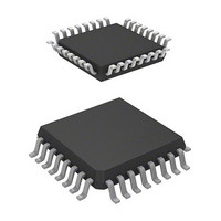
Manufacturer Part Number
DF36912GFH
Description
MCU 3/5V 8K 32-LQFP
Manufacturer
Renesas Electronics America
Series
H8® H8/300H Tinyr
Datasheet
1.DF36912GFHV.pdf
(442 pages)
Specifications of DF36912GFH
Core Processor
H8/300H
Core Size
16-Bit
Speed
12MHz
Connectivity
I²C, SCI
Peripherals
LVD, POR, PWM, WDT
Number Of I /o
18
Program Memory Size
8KB (8K x 8)
Program Memory Type
FLASH
Ram Size
1.5K x 8
Voltage - Supply (vcc/vdd)
3 V ~ 5.5 V
Data Converters
A/D 4x10b
Oscillator Type
Internal
Operating Temperature
-20°C ~ 75°C
Package / Case
32-LQFP
Lead Free Status / RoHS Status
Lead free / RoHS Compliant
Eeprom Size
-
Available stocks
Company
Part Number
Manufacturer
Quantity
Price
Company:

Part Number:
DF36912GFH
Manufacturer:
Renesas Electronics America
Quantity:
10 000
Company:
Part Number:
DF36912GFHV
Manufacturer:
Renesas Electronics America
Quantity:
10 000


Section 14 Serial Communication Interface 3 (SCI3)
14.5.2
Before transmitting and receiving data, SCI3 should be initialized as described in a sample
flowchart in figure 14.5.
14.5.3
Figure 14.11 shows an example of SCI3 operation for transmission in clocked synchronous mode.
In serial transmission, SCI3 operates as described below.
1. SCI3 monitors the TDRE flag in SSR, and if the flag is 0, SCI3 recognizes that data has been
2. SCI3 sets the TDRE flag to 1 and starts transmission. If the TIE bit in SCR3 is set to 1 at this
3. 8-bit data is sent from the TXD pin synchronized with the output clock when output clock
4. SCI3 checks the TDRE flag at the timing for sending the MSB (bit 7).
5. If the TDRE flag is cleared to 0, data is transferred from TDR to TSR, and serial transmission
6. If the TDRE flag is set to 1, the TEND flag in SSR is set to 1, and the TDRE flag maintains the
7. The SCK3 pin is fixed high at the end of transmission.
Rev. 3.00 Sep. 14, 2006 Page 220 of 408
REJ09B0105-0300
written to TDR, and transfers the data from TDR to TSR.
time, a transmit data empty interrupt (TXI) is generated.
mode has been specified, and synchronized with the input clock when use of an external clock
has been specified. Serial data is transmitted sequentially from the LSB (bit 0), from the TXD
pin.
of the next frame is started.
output state of the last bit. If the TEIE bit in SCR3 is set to 1 at this time, a TEI interrupt
request is generated.
SCI3 Initialization
Serial Data Transmission
Related parts for DF36912GFH
Image
Part Number
Description
Manufacturer
Datasheet
Request
R

Part Number:
Description:
Headers & Wire Housings 20P PLUG METAL COVER
Manufacturer:
Hirose Electric Co Ltd
Part Number:
Description:
Headers & Wire Housings 25P PLUG METAL COVER
Manufacturer:
Hirose Electric Co Ltd
Part Number:
Description:
Headers & Wire Housings 15P PLUG METAL COVER
Manufacturer:
Hirose Electric Co Ltd

Part Number:
Description:
0.4 Mm Pitch, 1.5 Mm Mated Height, Board-to-fine Coaxial Cable Connectors
Manufacturer:
Hirose Electric
Datasheet:
Part Number:
Description:
CONN RECEPT 40POS 0.4MM SMD GOLD
Manufacturer:
Hirose Electric Co Ltd
Datasheet:

Part Number:
Description:
KIT STARTER FOR M16C/29
Manufacturer:
Renesas Electronics America
Datasheet:

Part Number:
Description:
KIT STARTER FOR R8C/2D
Manufacturer:
Renesas Electronics America
Datasheet:

Part Number:
Description:
R0K33062P STARTER KIT
Manufacturer:
Renesas Electronics America
Datasheet:

Part Number:
Description:
KIT STARTER FOR R8C/23 E8A
Manufacturer:
Renesas Electronics America
Datasheet:

Part Number:
Description:
KIT STARTER FOR R8C/25
Manufacturer:
Renesas Electronics America
Datasheet:

Part Number:
Description:
KIT STARTER H8S2456 SHARPE DSPLY
Manufacturer:
Renesas Electronics America
Datasheet:

Part Number:
Description:
KIT STARTER FOR R8C38C
Manufacturer:
Renesas Electronics America
Datasheet:

Part Number:
Description:
KIT STARTER FOR R8C35C
Manufacturer:
Renesas Electronics America
Datasheet:

Part Number:
Description:
KIT STARTER FOR R8CL3AC+LCD APPS
Manufacturer:
Renesas Electronics America
Datasheet:
Part Number:
Description:
KIT STARTER FOR RX610
Manufacturer:
Renesas Electronics America
Datasheet: