DF36912GFH Renesas Electronics America, DF36912GFH Datasheet - Page 431
DF36912GFH
Manufacturer Part Number
DF36912GFH
Description
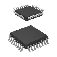
MCU 3/5V 8K 32-LQFP
Manufacturer
Renesas Electronics America
Series
H8® H8/300H Tinyr
Datasheet
1.DF36912GFHV.pdf
(442 pages)
Specifications of DF36912GFH
Core Processor
H8/300H
Core Size
16-Bit
Speed
12MHz
Connectivity
I²C, SCI
Peripherals
LVD, POR, PWM, WDT
Number Of I /o
18
Program Memory Size
8KB (8K x 8)
Program Memory Type
FLASH
Ram Size
1.5K x 8
Voltage - Supply (vcc/vdd)
3 V ~ 5.5 V
Data Converters
A/D 4x10b
Oscillator Type
Internal
Operating Temperature
-20°C ~ 75°C
Package / Case
32-LQFP
Lead Free Status / RoHS Status
Lead free / RoHS Compliant
Eeprom Size
-
Available stocks
Company
Part Number
Manufacturer
Quantity
Price
Company:

Part Number:
DF36912GFH
Manufacturer:
Renesas Electronics America
Quantity:
10 000
Company:
Part Number:
DF36912GFHV
Manufacturer:
Renesas Electronics America
Quantity:
10 000


Item
Figure 2.1 Memory Map (2)
Table 3.1 Exception Sources
and Vector Address
Figure 5.1 Block Diagram of
Clock Pulse Generators
5.2.1 RC Control Register
(RCCR)
5.2.2 RC Trimming Data
Protect Register
(RCTRMDPR)
Page Revision (See Manual for Details)
13
48
69
71
73
Bit
1
0
Bit
4
Note: * Available for the H8/36912 Group only.
Relative Module
IIC2*
Timer B1*
Bit Name
RCPSC1
RCPSC0
Bit Name
TRMDRWE Trimming Date Register Write Enable
H'0000
H'0045
H'0046
(Masked ROM version
(under planning))
OSC
OSC
Interrupt vector
oscillator
On-chip
Description
Division Ratio Select for On-chip Oscillator
The division ratio of R
rewriting this bit.
These bits can be written to only when the CKSTA
bit in CKCSR is 0.
0X: R
10: R
11: R
Description
This register can be written to when the LOCKDW
bit is 0 and this bit is 1.
[Setting condition]
[Clearing conditions]
H8/36911
H8/36901
1
2
When writing 0 to the WRI bit while writing 1 to
the TRMDRWE bit while the PRWE bit is 1
Reset
When writing 0 to the WRI bit and writing 0 to
the TRMDRWE bit while the PRWE bit is 1
OSC
OSC
Rev. 3.00 Sep. 14, 2006 Page 401 of 408
OSC
R
/2
OSC
/4
oscillator
(not divided)
Exception Sources
IIC_2 transmit data empty
IIC_2 transmit end
IIC_2 receive error
Timer B1 overflow
System
clock
divider
Clock
H'0000
H'0045
H'0046
OSC
R
R
R
OSC
OSC
OSC
OSC
(Masked ROM version
correction
circuit
/2
/4
Duty
(under planning))
changes right after
Interrupt vector
H8/36900
REJ09B0105-0300
Related parts for DF36912GFH
Image
Part Number
Description
Manufacturer
Datasheet
Request
R

Part Number:
Description:
Headers & Wire Housings 20P PLUG METAL COVER
Manufacturer:
Hirose Electric Co Ltd
Part Number:
Description:
Headers & Wire Housings 25P PLUG METAL COVER
Manufacturer:
Hirose Electric Co Ltd
Part Number:
Description:
Headers & Wire Housings 15P PLUG METAL COVER
Manufacturer:
Hirose Electric Co Ltd

Part Number:
Description:
0.4 Mm Pitch, 1.5 Mm Mated Height, Board-to-fine Coaxial Cable Connectors
Manufacturer:
Hirose Electric
Datasheet:
Part Number:
Description:
CONN RECEPT 40POS 0.4MM SMD GOLD
Manufacturer:
Hirose Electric Co Ltd
Datasheet:

Part Number:
Description:
KIT STARTER FOR M16C/29
Manufacturer:
Renesas Electronics America
Datasheet:

Part Number:
Description:
KIT STARTER FOR R8C/2D
Manufacturer:
Renesas Electronics America
Datasheet:

Part Number:
Description:
R0K33062P STARTER KIT
Manufacturer:
Renesas Electronics America
Datasheet:

Part Number:
Description:
KIT STARTER FOR R8C/23 E8A
Manufacturer:
Renesas Electronics America
Datasheet:

Part Number:
Description:
KIT STARTER FOR R8C/25
Manufacturer:
Renesas Electronics America
Datasheet:

Part Number:
Description:
KIT STARTER H8S2456 SHARPE DSPLY
Manufacturer:
Renesas Electronics America
Datasheet:

Part Number:
Description:
KIT STARTER FOR R8C38C
Manufacturer:
Renesas Electronics America
Datasheet:

Part Number:
Description:
KIT STARTER FOR R8C35C
Manufacturer:
Renesas Electronics America
Datasheet:

Part Number:
Description:
KIT STARTER FOR R8CL3AC+LCD APPS
Manufacturer:
Renesas Electronics America
Datasheet:
Part Number:
Description:
KIT STARTER FOR RX610
Manufacturer:
Renesas Electronics America
Datasheet: