DF36912GFH Renesas Electronics America, DF36912GFH Datasheet - Page 24
DF36912GFH
Manufacturer Part Number
DF36912GFH
Description
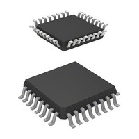
MCU 3/5V 8K 32-LQFP
Manufacturer
Renesas Electronics America
Series
H8® H8/300H Tinyr
Datasheet
1.DF36912GFHV.pdf
(442 pages)
Specifications of DF36912GFH
Core Processor
H8/300H
Core Size
16-Bit
Speed
12MHz
Connectivity
I²C, SCI
Peripherals
LVD, POR, PWM, WDT
Number Of I /o
18
Program Memory Size
8KB (8K x 8)
Program Memory Type
FLASH
Ram Size
1.5K x 8
Voltage - Supply (vcc/vdd)
3 V ~ 5.5 V
Data Converters
A/D 4x10b
Oscillator Type
Internal
Operating Temperature
-20°C ~ 75°C
Package / Case
32-LQFP
Lead Free Status / RoHS Status
Lead free / RoHS Compliant
Eeprom Size
-
Available stocks
Company
Part Number
Manufacturer
Quantity
Price
Company:

Part Number:
DF36912GFH
Manufacturer:
Renesas Electronics America
Quantity:
10 000
Company:
Part Number:
DF36912GFHV
Manufacturer:
Renesas Electronics America
Quantity:
10 000


Section 13 Watchdog Timer
Figure 13.1 Block Diagram of Watchdog Timer ........................................................................ 191
Figure 13.2 Watchdog Timer Operation Example...................................................................... 195
Section 14 Serial Communication Interface 3 (SCI3)
Figure 14.1 Block Diagram of SCI3........................................................................................... 198
Figure 14.2 Block Diagram of Noise Filter Circuit .................................................................... 211
Figure 14.3 Data Format in Asynchronous Communication ...................................................... 212
Figure 14.4 Relationship between Output Clock and Transfer Data Phase
Figure 14.5 Sample SCI3 Initialization Flowchart ..................................................................... 213
Figure 14.6 Example of SCI3 Transmission in Asynchronous Mode
Figure 14.7 Sample Serial Transmission Data Flowchart (Asynchronous Mode)...................... 215
Figure 14.8 Example of SCI3 Reception in Asynchronous Mode
Figure 14.9 Sample Serial Reception Data Flowchart (Asynchronous Mode) ........................... 218
Figure 14.10 Data Format in Clocked Synchronous Communication ........................................ 219
Figure 14.11 Example of SCI3 Transmission in Clocked Synchronous Mode .......................... 221
Figure 14.12 Sample Serial Transmission Flowchart (Clocked Synchronous Mode) ................ 222
Figure 14.13 Example of SCI3 Reception in Clocked Synchronous Mode................................ 223
Figure 14.14 Sample Serial Reception Flowchart (Clocked Synchronous Mode)...................... 224
Figure 14.15 Sample Flowchart of Simultaneous Serial Transmit and Receive Operations
Figure 14.16 Example of Inter-Processor Communication Using Multiprocessor Format
Figure 14.17 Sample Multiprocessor Serial Transmission Flowchart ........................................ 230
Figure 14.18 Sample Multiprocessor Serial Reception Flowchart (1)........................................ 232
Figure 14.18 Sample Multiprocessor Serial Reception Flowchart (2)........................................ 233
Figure 14.19 Example of SCI3 Reception Using Multiprocessor Format
Figure 14.20 Receive Data Sampling Timing in Asynchronous Mode ...................................... 237
Section 15 I
Figure 15.1 Block Diagram of I
Figure 15.2 External Circuit Connections of I/O Pins ................................................................ 241
Figure 15.3 I
Figure 15.4 I
Figure 15.5 Master Transmit Mode Operation Timing (1)......................................................... 256
Figure 15.6 Master Transmit Mode Operation Timing (2)......................................................... 256
Figure 15.7 Master Receive Mode Operation Timing (1) .......................................................... 258
Rev. 3.00 Sep. 14, 2006 Page xxii of xxviii
(Asynchronous Mode) (Example with 8-Bit Data, Parity, Two Stop Bits) ............. 212
(8-Bit Data, Parity, One Stop Bit) ........................................................................... 214
(8-Bit Data, Parity, One Stop Bit) ........................................................................... 216
2
2
2
C Bus Interface 2 (IIC2)
(Clocked Synchronous Mode)............................................................................... 226
(Transmission of Data H'AA to Receiving Station A) .......................................... 228
(Example with 8-Bit Data, Multiprocessor Bit, One Stop Bit).............................. 234
C Bus Formats ...................................................................................................... 254
C Bus Timing........................................................................................................ 254
2
C Bus Interface 2..................................................................... 240
Related parts for DF36912GFH
Image
Part Number
Description
Manufacturer
Datasheet
Request
R

Part Number:
Description:
Headers & Wire Housings 20P PLUG METAL COVER
Manufacturer:
Hirose Electric Co Ltd
Part Number:
Description:
Headers & Wire Housings 25P PLUG METAL COVER
Manufacturer:
Hirose Electric Co Ltd
Part Number:
Description:
Headers & Wire Housings 15P PLUG METAL COVER
Manufacturer:
Hirose Electric Co Ltd

Part Number:
Description:
0.4 Mm Pitch, 1.5 Mm Mated Height, Board-to-fine Coaxial Cable Connectors
Manufacturer:
Hirose Electric
Datasheet:
Part Number:
Description:
CONN RECEPT 40POS 0.4MM SMD GOLD
Manufacturer:
Hirose Electric Co Ltd
Datasheet:

Part Number:
Description:
KIT STARTER FOR M16C/29
Manufacturer:
Renesas Electronics America
Datasheet:

Part Number:
Description:
KIT STARTER FOR R8C/2D
Manufacturer:
Renesas Electronics America
Datasheet:

Part Number:
Description:
R0K33062P STARTER KIT
Manufacturer:
Renesas Electronics America
Datasheet:

Part Number:
Description:
KIT STARTER FOR R8C/23 E8A
Manufacturer:
Renesas Electronics America
Datasheet:

Part Number:
Description:
KIT STARTER FOR R8C/25
Manufacturer:
Renesas Electronics America
Datasheet:

Part Number:
Description:
KIT STARTER H8S2456 SHARPE DSPLY
Manufacturer:
Renesas Electronics America
Datasheet:

Part Number:
Description:
KIT STARTER FOR R8C38C
Manufacturer:
Renesas Electronics America
Datasheet:

Part Number:
Description:
KIT STARTER FOR R8C35C
Manufacturer:
Renesas Electronics America
Datasheet:

Part Number:
Description:
KIT STARTER FOR R8CL3AC+LCD APPS
Manufacturer:
Renesas Electronics America
Datasheet:
Part Number:
Description:
KIT STARTER FOR RX610
Manufacturer:
Renesas Electronics America
Datasheet: