DF36912GFH Renesas Electronics America, DF36912GFH Datasheet - Page 433
DF36912GFH
Manufacturer Part Number
DF36912GFH
Description
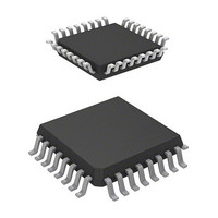
MCU 3/5V 8K 32-LQFP
Manufacturer
Renesas Electronics America
Series
H8® H8/300H Tinyr
Datasheet
1.DF36912GFHV.pdf
(442 pages)
Specifications of DF36912GFH
Core Processor
H8/300H
Core Size
16-Bit
Speed
12MHz
Connectivity
I²C, SCI
Peripherals
LVD, POR, PWM, WDT
Number Of I /o
18
Program Memory Size
8KB (8K x 8)
Program Memory Type
FLASH
Ram Size
1.5K x 8
Voltage - Supply (vcc/vdd)
3 V ~ 5.5 V
Data Converters
A/D 4x10b
Oscillator Type
Internal
Operating Temperature
-20°C ~ 75°C
Package / Case
32-LQFP
Lead Free Status / RoHS Status
Lead free / RoHS Compliant
Eeprom Size
-
Available stocks
Company
Part Number
Manufacturer
Quantity
Price
Company:

Part Number:
DF36912GFH
Manufacturer:
Renesas Electronics America
Quantity:
10 000
Company:
Part Number:
DF36912GFHV
Manufacturer:
Renesas Electronics America
Quantity:
10 000


Item
13.2.1 Timer Control/Status
Register WD (TCSRWD)
14.8.2 Mark State and Break
Sending
15.3.5 I
Register (ICSR)
Figure 15.15 Receive Mode
Operation Timing
15.7 Usage Notes
16.3.1 A/D Data Registers A
to D (ADDRA to ADDRD)
Figure 17.2 Block Diagram
of Power-On Reset Circuit
and Low-Voltage Detection
Circuit
20.3 Electrical
Characteristics (Masked
ROM Version)
2
C Bus Status
Page Revision (See Manual for Details)
192
236
251
265
272
276
287
331
Replaced
Added
There are four 16-bit read-only ADDR registers; ……
Therefore, byte access to ADDR should be done by reading the
upper byte first then the lower one. ADDR is initialized to H'0000.
20.3 Electrical Characteristics (Masked ROM Version) [Preliminary]
The guarantee value for the electrical characteristics of masked ROM
version is preliminary.
20.3.1 Power Supply Voltage and Operating Ranges
Bit
4
Bit
3
Bit Name Description
TCSRWE Timer Control/Status Register WD Write Enable
Bit Name Description
STOP
(Input)
SDA
MST
SCL
The WDON and WRST bits can be written when
the TCSRWE bit is set to 1.
When writing data to this bit, the value for bit 5
must be 0.
Stop Condition Detection Flag
[Setting conditions]
……
In master mode, when a stop condition is
detected after frame transfer
In slave mode, when a stop condition is
detected after the general call address or
the first byte slave address, next to
detection of start condition, accords with the
address set in SAR
Rev. 3.00 Sep. 14, 2006 Page 403 of 408
C
RES
Bit 6
7
RES
Bit 7
8
Bit 0
1
REJ09B0105-0300
Bit 1
2
Related parts for DF36912GFH
Image
Part Number
Description
Manufacturer
Datasheet
Request
R

Part Number:
Description:
Headers & Wire Housings 20P PLUG METAL COVER
Manufacturer:
Hirose Electric Co Ltd
Part Number:
Description:
Headers & Wire Housings 25P PLUG METAL COVER
Manufacturer:
Hirose Electric Co Ltd
Part Number:
Description:
Headers & Wire Housings 15P PLUG METAL COVER
Manufacturer:
Hirose Electric Co Ltd

Part Number:
Description:
0.4 Mm Pitch, 1.5 Mm Mated Height, Board-to-fine Coaxial Cable Connectors
Manufacturer:
Hirose Electric
Datasheet:
Part Number:
Description:
CONN RECEPT 40POS 0.4MM SMD GOLD
Manufacturer:
Hirose Electric Co Ltd
Datasheet:

Part Number:
Description:
KIT STARTER FOR M16C/29
Manufacturer:
Renesas Electronics America
Datasheet:

Part Number:
Description:
KIT STARTER FOR R8C/2D
Manufacturer:
Renesas Electronics America
Datasheet:

Part Number:
Description:
R0K33062P STARTER KIT
Manufacturer:
Renesas Electronics America
Datasheet:

Part Number:
Description:
KIT STARTER FOR R8C/23 E8A
Manufacturer:
Renesas Electronics America
Datasheet:

Part Number:
Description:
KIT STARTER FOR R8C/25
Manufacturer:
Renesas Electronics America
Datasheet:

Part Number:
Description:
KIT STARTER H8S2456 SHARPE DSPLY
Manufacturer:
Renesas Electronics America
Datasheet:

Part Number:
Description:
KIT STARTER FOR R8C38C
Manufacturer:
Renesas Electronics America
Datasheet:

Part Number:
Description:
KIT STARTER FOR R8C35C
Manufacturer:
Renesas Electronics America
Datasheet:

Part Number:
Description:
KIT STARTER FOR R8CL3AC+LCD APPS
Manufacturer:
Renesas Electronics America
Datasheet:
Part Number:
Description:
KIT STARTER FOR RX610
Manufacturer:
Renesas Electronics America
Datasheet: