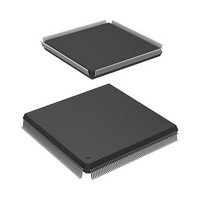
HD6417727F100C Renesas Electronics America, HD6417727F100C Datasheet - Page 825

HD6417727F100C
Manufacturer Part Number
HD6417727F100C
Description
IC SUPERH MPU ROMLESS 240QFP
Manufacturer
Renesas Electronics America
Series
SuperH® SH7700r
Datasheet
1.HD6417727BP100CV.pdf
(1098 pages)
Specifications of HD6417727F100C
Core Processor
SH-3 DSP
Core Size
32-Bit
Speed
100MHz
Connectivity
FIFO, SCI, SIO, SmartCard, USB
Peripherals
DMA, LCD, POR, WDT
Number Of I /o
104
Program Memory Type
ROMless
Ram Size
32K x 8
Voltage - Supply (vcc/vdd)
1.6 V ~ 2.05 V
Data Converters
A/D 6x10b; D/A 2x8b
Oscillator Type
Internal
Operating Temperature
-20°C ~ 75°C
Package / Case
240-QFP
Lead Free Status / RoHS Status
Contains lead / RoHS non-compliant
Eeprom Size
-
Program Memory Size
-
Available stocks
Company
Part Number
Manufacturer
Quantity
Price
Company:
Part Number:
HD6417727F100C
Manufacturer:
Renesas Electronics America
Quantity:
10 000
- Current page: 825 of 1098
- Download datasheet (7Mb)
25.2
25.2.1
This LCDC can select the bus clock (Bφ), the peripheral clock (Pφ), or the external clock as its
operation clock source. The selected clock source can be divided using an internal divider into a
clock of 1/1 to 1/16 and be used as the LCDC operating clock (DOTCLOCK). The clock output
from the LCDC is used to generate the synchronous clock output (CL2) for the LCD panel from
the operating clock selected in this register. The average frequency of CL2 can be calculated using
the formula below. The actual frequency, however, will differ depending on the type of LCD panel
and the bus width of the data output to the LCD panel. See section 25.4, Clock and LCD Data
Signal Examples, for details.
Set this register so that the clock input to the LCDC is 50 MHz or less regardless of CL2.
Bits 15, 14, and 11 to 5—Reserved
Bits 13 and 12—Input Clock Select (ICKSEL1 and ICKSEL0): Set the clock source for
DOTCLOCK.
Bit 13
ICKSEL1
0
1
Initial value:
TFT panel
STN or DSTN panel
R/W:
Bit:
CL2 = DOTCLOCK
Monochrome: CL2 = (DOTCLOCK/data bus width of output to LCD panel)
Color: CL2 = 3 × (DOTCLOCK/data bus width of output to LCD panel)
Register Descriptions
LCDC Input Clock Register (LDICKR)
15
—
R
0
Bit 12
ICKSEL0
1
1
0
0
14
—
R
0
ICKSEL
R/W
13
1
0
Description
Bus clock (Bφ) is selected
Peripheral clock (Pφ) is selected
External clock (LCLK) is selected
Reserved (setting prohibited)
ICKSEL
R/W
12
0
0
11
—
R
0
10
—
R
0
—
R
9
0
—
R
8
1
Rev.6.00 Mar. 27, 2009 Page 767 of 1036
—
R
0
7
—
R
6
0
—
R
5
0
DCDR4 DCDR3 DCDR2 DCDR1 DCDR0
Section 25 LCD Controller
R/W
4
0
R/W
3
0
REJ09B0254-0600
R/W
2
0
(Initial value)
R/W
1
0
R/W
0
1
Related parts for HD6417727F100C
Image
Part Number
Description
Manufacturer
Datasheet
Request
R

Part Number:
Description:
KIT STARTER FOR M16C/29
Manufacturer:
Renesas Electronics America
Datasheet:

Part Number:
Description:
KIT STARTER FOR R8C/2D
Manufacturer:
Renesas Electronics America
Datasheet:

Part Number:
Description:
R0K33062P STARTER KIT
Manufacturer:
Renesas Electronics America
Datasheet:

Part Number:
Description:
KIT STARTER FOR R8C/23 E8A
Manufacturer:
Renesas Electronics America
Datasheet:

Part Number:
Description:
KIT STARTER FOR R8C/25
Manufacturer:
Renesas Electronics America
Datasheet:

Part Number:
Description:
KIT STARTER H8S2456 SHARPE DSPLY
Manufacturer:
Renesas Electronics America
Datasheet:

Part Number:
Description:
KIT STARTER FOR R8C38C
Manufacturer:
Renesas Electronics America
Datasheet:

Part Number:
Description:
KIT STARTER FOR R8C35C
Manufacturer:
Renesas Electronics America
Datasheet:

Part Number:
Description:
KIT STARTER FOR R8CL3AC+LCD APPS
Manufacturer:
Renesas Electronics America
Datasheet:

Part Number:
Description:
KIT STARTER FOR RX610
Manufacturer:
Renesas Electronics America
Datasheet:

Part Number:
Description:
KIT STARTER FOR R32C/118
Manufacturer:
Renesas Electronics America
Datasheet:

Part Number:
Description:
KIT DEV RSK-R8C/26-29
Manufacturer:
Renesas Electronics America
Datasheet:

Part Number:
Description:
KIT STARTER FOR SH7124
Manufacturer:
Renesas Electronics America
Datasheet:

Part Number:
Description:
KIT STARTER FOR H8SX/1622
Manufacturer:
Renesas Electronics America
Datasheet:

Part Number:
Description:
KIT DEV FOR SH7203
Manufacturer:
Renesas Electronics America
Datasheet:


