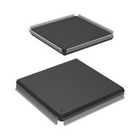
HD6417727F100C Renesas Electronics America, HD6417727F100C Datasheet - Page 83

HD6417727F100C
Manufacturer Part Number
HD6417727F100C
Description
IC SUPERH MPU ROMLESS 240QFP
Manufacturer
Renesas Electronics America
Series
SuperH® SH7700r
Datasheet
1.HD6417727BP100CV.pdf
(1098 pages)
Specifications of HD6417727F100C
Core Processor
SH-3 DSP
Core Size
32-Bit
Speed
100MHz
Connectivity
FIFO, SCI, SIO, SmartCard, USB
Peripherals
DMA, LCD, POR, WDT
Number Of I /o
104
Program Memory Type
ROMless
Ram Size
32K x 8
Voltage - Supply (vcc/vdd)
1.6 V ~ 2.05 V
Data Converters
A/D 6x10b; D/A 2x8b
Oscillator Type
Internal
Operating Temperature
-20°C ~ 75°C
Package / Case
240-QFP
Lead Free Status / RoHS Status
Contains lead / RoHS non-compliant
Eeprom Size
-
Program Memory Size
-
Available stocks
Company
Part Number
Manufacturer
Quantity
Price
Company:
Part Number:
HD6417727F100C
Manufacturer:
Renesas Electronics America
Quantity:
10 000
- Current page: 83 of 1098
- Download datasheet (7Mb)
2.1.1
There are sixteen 32-bit general registers (Rn), designated R0 to R15. The general registers are
used for data processing and address calculation.
With SuperH microcomputer type instructions, R0 is used as an index register. With a number of
instructions, R0 is the only register that can be used. R15 is used as the stack pointer (SP). In
exception handling, R15 is used to reference the stack when saving and restoring the status register
(SR) and program counter (PC).
With DSP type instructions, eight of the sixteen general registers are used for addressing of X and
Y data memory and data memory (single data) that uses the L-bus.
To access X memory, R4 and R5 are used as X address register [Ax] and R8 is used as X index
register [Ix]. To access Y memory, R6 and R7 are used as Y address register [Ay] and R9 is used
as Y index register [Iy]. To access single data that uses the L-bus, R2, R3, R4, and R5 are used as
single data address register [As] and R8 is used as single data index register [Is].
Figure 2.3 shows the general purpose registers, which are identical to SH-3’s, when DSP
extension is disabled.
31
General Purpose Registers
R0
R1
R2
R3
R4
R5
R6
R7
R8
R9
R10
R11
R12
R13
R14
R15
Figure 2.3 General Purpose Register (Not in DSP Mode)
*1 *2
*2
*2
*2
*2
*2
*2
*2
0
General Registers (when not in DSP mode)
Notes: 1. R0 functions as an index register in the
2. R0 to R7 are banked registers. In user mode,
indexed register-indirect addressing mode
and indexed GBR-indirect addressing mode.
In some instructions, only R0 can be used as
the source register or destination register.
BANK0 is used. In privileged mode, SR.RB
specifies BANK.
SR.RB = 0; BANK0 is used
SR.RB = 1; BANK1 is used
Rev.6.00 Mar. 27, 2009 Page 25 of 1036
REJ09B0254-0600
Section 2 CPU
Related parts for HD6417727F100C
Image
Part Number
Description
Manufacturer
Datasheet
Request
R

Part Number:
Description:
KIT STARTER FOR M16C/29
Manufacturer:
Renesas Electronics America
Datasheet:

Part Number:
Description:
KIT STARTER FOR R8C/2D
Manufacturer:
Renesas Electronics America
Datasheet:

Part Number:
Description:
R0K33062P STARTER KIT
Manufacturer:
Renesas Electronics America
Datasheet:

Part Number:
Description:
KIT STARTER FOR R8C/23 E8A
Manufacturer:
Renesas Electronics America
Datasheet:

Part Number:
Description:
KIT STARTER FOR R8C/25
Manufacturer:
Renesas Electronics America
Datasheet:

Part Number:
Description:
KIT STARTER H8S2456 SHARPE DSPLY
Manufacturer:
Renesas Electronics America
Datasheet:

Part Number:
Description:
KIT STARTER FOR R8C38C
Manufacturer:
Renesas Electronics America
Datasheet:

Part Number:
Description:
KIT STARTER FOR R8C35C
Manufacturer:
Renesas Electronics America
Datasheet:

Part Number:
Description:
KIT STARTER FOR R8CL3AC+LCD APPS
Manufacturer:
Renesas Electronics America
Datasheet:

Part Number:
Description:
KIT STARTER FOR RX610
Manufacturer:
Renesas Electronics America
Datasheet:

Part Number:
Description:
KIT STARTER FOR R32C/118
Manufacturer:
Renesas Electronics America
Datasheet:

Part Number:
Description:
KIT DEV RSK-R8C/26-29
Manufacturer:
Renesas Electronics America
Datasheet:

Part Number:
Description:
KIT STARTER FOR SH7124
Manufacturer:
Renesas Electronics America
Datasheet:

Part Number:
Description:
KIT STARTER FOR H8SX/1622
Manufacturer:
Renesas Electronics America
Datasheet:

Part Number:
Description:
KIT DEV FOR SH7203
Manufacturer:
Renesas Electronics America
Datasheet:


