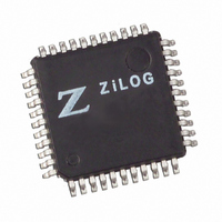
Z8F6401AN020SC00TR Zilog, Z8F6401AN020SC00TR Datasheet - Page 160

Z8F6401AN020SC00TR
Manufacturer Part Number
Z8F6401AN020SC00TR
Description
IC ENCORE MCU FLASH 64K 44LQFP
Manufacturer
Zilog
Series
Encore!®r
Datasheet
1.Z8F1601VN020EC.pdf
(246 pages)
Specifications of Z8F6401AN020SC00TR
Core Processor
Z8
Core Size
8-Bit
Speed
20MHz
Connectivity
I²C, IrDA, SPI, UART/USART
Peripherals
Brown-out Detect/Reset, DMA, POR, PWM, WDT
Number Of I /o
31
Program Memory Size
64KB (64K x 8)
Program Memory Type
FLASH
Ram Size
4K x 8
Voltage - Supply (vcc/vdd)
3 V ~ 3.6 V
Data Converters
A/D 8x10b
Oscillator Type
Internal
Operating Temperature
0°C ~ 70°C
Package / Case
44-LQFP
Lead Free Status / RoHS Status
Contains lead / RoHS non-compliant
Eeprom Size
-
Other names
Z8F6401AN020SC00T
Available stocks
Company
Part Number
Manufacturer
Quantity
Price
- Current page: 160 of 246
- Download datasheet (2Mb)
PS017610-0404
Byte Programming
Flash Code Protection Using the Option Bits
The FHSWP and FWP Option Bits combine to provide three levels of Flash Program Mem-
ory protection as listed in Table 84. Refer to the Option Bits chapter for more informa-
tion.
Table 84. Flash Code Protection Using the Option Bits
Flash Code Protection Using the Flash Controller
At Reset, the Flash Controller locks to prevent accidental program or erasure of the Flash
memory. To program or erase the Flash memory, unlock the Flash Controller by making
two consecutive writes to the Flash Control register with the values
tially. After unlocking the Flash Controller, the Flash can be programmed or erased. When
the Flash Controller is unlocked, any value written to the Flash Control register locks the
Flash Controller. Writing the Mass Erase or Page Erase commands executes the function
before locking the Flash Controller.
When the Flash Controller is unlocked, all writes to Program Memory program a byte into
the Flash. An erased Flash byte contains all 1’s (
only be used to change bits from 1 to 0. To change a Flash bit (or multiple bits) from 0 to 1
requires execution of either the Page Erase or Mass Erase commands.
Byte Programming can be accomplished using the On-Chip Debugger's Write Memory
command or eZ8 CPU execution of the LDC or LDCI instructions. Refer to the eZ8 CPU
User Manual for a description of the LDC and LDCI instructions. While the Flash Con-
troller programs the Flash memory, the eZ8 CPU idles but the system clock and on-chip
peripherals continue to operate. To exit programming mode and lock the Flash, write any
value to the Flash Control register, except the Mass Erase or Page Erase commands.
FHSWP
0 or 1
0
1
FWP
0
0
1
Flash Code Protection Description
Programming and erasure disabled for all of Flash Program Memory. In
user code programming, Page Erase, and Mass Erase are all disabled. Mass
Erase is available through the On-Chip Debugger.
Programming and Page Erase are enabled for the High Sector of the Flash
Program Memory only. The High Sector on the Z8F640x family device
contains 1KB to 4KB of Flash with addresses at the top of the available
Flash memory. Programming and Page Erase are disabled for the other
portions of the Flash Program Memory. Mass erase through user code is
disabled. Mass Erase is available through the On-Chip Debugger.
Programming, Page Erase, and Mass Erase are enabled for all of Flash
Program Memory.
Z8F640x/Z8F480x/Z8F320x/Z8F240x/Z8F160x
FFH
). The programming operation can
73H
and
Z8 Encore!
Flash Memory
8CH
, sequen-
®
142
Related parts for Z8F6401AN020SC00TR
Image
Part Number
Description
Manufacturer
Datasheet
Request
R

Part Number:
Description:
Communication Controllers, ZILOG INTELLIGENT PERIPHERAL CONTROLLER (ZIP)
Manufacturer:
Zilog, Inc.
Datasheet:

Part Number:
Description:
KIT DEV FOR Z8 ENCORE 16K TO 64K
Manufacturer:
Zilog
Datasheet:

Part Number:
Description:
KIT DEV Z8 ENCORE XP 28-PIN
Manufacturer:
Zilog
Datasheet:

Part Number:
Description:
DEV KIT FOR Z8 ENCORE 8K/4K
Manufacturer:
Zilog
Datasheet:

Part Number:
Description:
KIT DEV Z8 ENCORE XP 28-PIN
Manufacturer:
Zilog
Datasheet:

Part Number:
Description:
DEV KIT FOR Z8 ENCORE 4K TO 8K
Manufacturer:
Zilog
Datasheet:

Part Number:
Description:
CMOS Z8 microcontroller. ROM 16 Kbytes, RAM 256 bytes, speed 16 MHz, 32 lines I/O, 3.0V to 5.5V
Manufacturer:
Zilog, Inc.
Datasheet:

Part Number:
Description:
Low-cost microcontroller. 512 bytes ROM, 61 bytes RAM, 8 MHz
Manufacturer:
Zilog, Inc.
Datasheet:

Part Number:
Description:
Z8 4K OTP Microcontroller
Manufacturer:
Zilog, Inc.
Datasheet:

Part Number:
Description:
CMOS SUPER8 ROMLESS MCU
Manufacturer:
Zilog, Inc.
Datasheet:

Part Number:
Description:
SL1866 CMOSZ8 OTP Microcontroller
Manufacturer:
Zilog, Inc.
Datasheet:

Part Number:
Description:
SL1866 CMOSZ8 OTP Microcontroller
Manufacturer:
Zilog, Inc.
Datasheet:

Part Number:
Description:
OTP (KB) = 1, RAM = 125, Speed = 12, I/O = 14, 8-bit Timers = 2, Comm Interfaces Other Features = Por, LV Protect, Voltage = 4.5-5.5V
Manufacturer:
Zilog, Inc.
Datasheet:

Part Number:
Description:
Manufacturer:
Zilog, Inc.
Datasheet:


