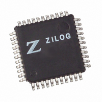
Z8F6401AN020SC00TR Zilog, Z8F6401AN020SC00TR Datasheet - Page 32

Z8F6401AN020SC00TR
Manufacturer Part Number
Z8F6401AN020SC00TR
Description
IC ENCORE MCU FLASH 64K 44LQFP
Manufacturer
Zilog
Series
Encore!®r
Datasheet
1.Z8F1601VN020EC.pdf
(246 pages)
Specifications of Z8F6401AN020SC00TR
Core Processor
Z8
Core Size
8-Bit
Speed
20MHz
Connectivity
I²C, IrDA, SPI, UART/USART
Peripherals
Brown-out Detect/Reset, DMA, POR, PWM, WDT
Number Of I /o
31
Program Memory Size
64KB (64K x 8)
Program Memory Type
FLASH
Ram Size
4K x 8
Voltage - Supply (vcc/vdd)
3 V ~ 3.6 V
Data Converters
A/D 8x10b
Oscillator Type
Internal
Operating Temperature
0°C ~ 70°C
Package / Case
44-LQFP
Lead Free Status / RoHS Status
Contains lead / RoHS non-compliant
Eeprom Size
-
Other names
Z8F6401AN020SC00T
Available stocks
Company
Part Number
Manufacturer
Quantity
Price
- Current page: 32 of 246
- Download datasheet (2Mb)
Table 2. Signal Descriptions (Continued)
PS017610-0404
Signal Mnemonic
UART Controllers
TXD0 / TXD1
RXD0 / RXD1
CTS0 / CTS1
Timers (Timer 3 is unavailable in the 40-and 44-pin packages)
T0OUT / T1OUT/
T2OUT / T3OUT
T0IN / T1IN/
T2IN / T3IN
Analog
ANA[11:0]
VREF
Oscillators
XIN
XOUT
RCOUT
On-Chip Debugger
DBG
I/O
I/O
O
O
O
O
I
I
I
I
I
I
Description
Transmit Data. These signals are the transmit outputs from the UARTs. The TXD
signals are multiplexed with general-purpose I/O pins.
Receive Data. These signals are the receiver inputs for the UARTs and IrDAs. The
RXD signals are multiplexed with general-purpose I/O pins.
Clear To Send. These signals are control inputs for the UARTs. The CTS signals
are multiplexed with general-purpose I/O pins.
Timer Output 0-3. These signals are output pins from the timers. The Timer
Output signals are multiplexed with general-purpose I/O pins. T2OUT is not
supported in the 40-pin package. T3OUT is not supported in the 40- and 44-pin
packages.
Timer Input 0-3. These signals are used as the capture, gating and counter inputs.
The Timer Input signals are multiplexed with general-purpose I/O pins. T3IN is
not supported in the 40- and 44-pin packages.
Analog Input. These signals are inputs to the analog-to-digital converter (ADC).
The ADC analog inputs are multiplexed with general-purpose I/O pins.
Analog-to-digital converter reference voltage input. The VREF pin should be left
unconnected (or capacitively coupled to analog ground) if the internal voltage
reference is selected as the ADC reference voltage.
External Crystal Input. This is the input pin to the crystal oscillator. A crystal can
be connected between it and the
External Crystal Output. This pin is the output of the crystal oscillator. A crystal
can be connected between it and the
system clock is referred to in this manual, it refers to the frequency of the signal at
this pin.
RC Oscillator Output. This signal is the output of the RC oscillator. It is
multiplexed with a general-purpose I/O pin.
Debug. This pin is the control and data input and output to and from the On-Chip
Debugger. For operation of the On-chip debugger, all power pins (V
must be supplied with power, and all ground pins (V
grounded. This pin is open-drain and must have an external pull-up resistor to
ensure proper operation.
Z8F640x/Z8F480x/Z8F320x/Z8F240x/Z8F160x
XOUT
XIN
pin to form the oscillator.
pin to form the oscillator. When the
Signal and Pin Descriptions
SS
and AV
SS
must be
Z8 Encore!
DD
and AV
DD
®
14
Related parts for Z8F6401AN020SC00TR
Image
Part Number
Description
Manufacturer
Datasheet
Request
R

Part Number:
Description:
Communication Controllers, ZILOG INTELLIGENT PERIPHERAL CONTROLLER (ZIP)
Manufacturer:
Zilog, Inc.
Datasheet:

Part Number:
Description:
KIT DEV FOR Z8 ENCORE 16K TO 64K
Manufacturer:
Zilog
Datasheet:

Part Number:
Description:
KIT DEV Z8 ENCORE XP 28-PIN
Manufacturer:
Zilog
Datasheet:

Part Number:
Description:
DEV KIT FOR Z8 ENCORE 8K/4K
Manufacturer:
Zilog
Datasheet:

Part Number:
Description:
KIT DEV Z8 ENCORE XP 28-PIN
Manufacturer:
Zilog
Datasheet:

Part Number:
Description:
DEV KIT FOR Z8 ENCORE 4K TO 8K
Manufacturer:
Zilog
Datasheet:

Part Number:
Description:
CMOS Z8 microcontroller. ROM 16 Kbytes, RAM 256 bytes, speed 16 MHz, 32 lines I/O, 3.0V to 5.5V
Manufacturer:
Zilog, Inc.
Datasheet:

Part Number:
Description:
Low-cost microcontroller. 512 bytes ROM, 61 bytes RAM, 8 MHz
Manufacturer:
Zilog, Inc.
Datasheet:

Part Number:
Description:
Z8 4K OTP Microcontroller
Manufacturer:
Zilog, Inc.
Datasheet:

Part Number:
Description:
CMOS SUPER8 ROMLESS MCU
Manufacturer:
Zilog, Inc.
Datasheet:

Part Number:
Description:
SL1866 CMOSZ8 OTP Microcontroller
Manufacturer:
Zilog, Inc.
Datasheet:

Part Number:
Description:
SL1866 CMOSZ8 OTP Microcontroller
Manufacturer:
Zilog, Inc.
Datasheet:

Part Number:
Description:
OTP (KB) = 1, RAM = 125, Speed = 12, I/O = 14, 8-bit Timers = 2, Comm Interfaces Other Features = Por, LV Protect, Voltage = 4.5-5.5V
Manufacturer:
Zilog, Inc.
Datasheet:

Part Number:
Description:
Manufacturer:
Zilog, Inc.
Datasheet:


