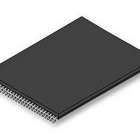
S29GL256P11TFI010 Spansion Inc., S29GL256P11TFI010 Datasheet - Page 3

S29GL256P11TFI010
Manufacturer Part Number
S29GL256P11TFI010
Description
Flash 3V 256Mb Mirrorbit highest address110ns
Manufacturer
Spansion Inc.
Specifications of S29GL256P11TFI010
Memory Type
NOR
Memory Size
256 Mbit
Access Time
110 ns
Data Bus Width
8 bit, 16 bit
Architecture
Uniform
Interface Type
Page-mode
Supply Voltage (max)
3.6 V
Supply Voltage (min)
2.7 V
Maximum Operating Current
50 mA
Mounting Style
SMD/SMT
Operating Temperature
+ 85 C
Package / Case
TSOP-56
Memory Configuration
128K X 16
Ic Interface Type
Parallel
Supply Voltage Range
2.7V To 3.6V
Memory Case Style
TSOP
No. Of Pins
56
Lead Free Status / RoHS Status
Lead free / RoHS Compliant
Lead Free Status / RoHS Status
Lead free / RoHS Compliant, Lead free / RoHS Compliant
Available stocks
Company
Part Number
Manufacturer
Quantity
Price
Company:
Part Number:
S29GL256P11TFI010
Manufacturer:
SPANSION
Quantity:
5 530
Company:
Part Number:
S29GL256P11TFI010
Manufacturer:
SPANSION
Quantity:
72
General Description
Distinctive Characteristics
Performance Characteristics
This document contains information on one or more products under development at Spansion Inc. The information is intended to help you evaluate this product. Do not design in
this product without contacting the factory. Spansion Inc. reserves the right to change or discontinue work on this proposed product without notice.
The Spansion S29GL01G/512/256/128P are Mirrorbit™ Flash products fabricated on 90 nm process technology. These
devices offer a fast page access time of 25 ns with a corresponding random access time of 110 ns. They feature a Write Buffer
that allows a maximum of 32 words/64 bytes to be programmed in one operation, resulting in faster effective programming time
than standard programming algorithms. This makes these devices ideal for today’s embedded applications that require higher
density, better performance and lower power consumption.
* Access times are dependent on V
** Contact a sales representative for availability.
S29GL-P MirrorBit
S29GL01GP, S29GL512P, S29GL256P, S29GL128P
1 Gigabit, 512 Megabit , 256 Megabit and 128 Megabit
3.0 Volt-only Page Mode Flash Memory featuring
90 nm MirrorBit Process Technology
Data Sheet (Advance Information)
Parameter
Random Access Time (t
Page Access Time (t
CE# Access Time (t
OE# Access Time (t
See
V1: V
V3: V
Single 3V read/program/erase (2.7-3.6 V)
Enhanced VersatileI/O™ control
– All input levels (address, control, and DQ input levels) and outputs
90 nm MirrorBit process technology
8-word/16-byte page read buffer
32-word/64-byte write buffer reduces overall programming
time for multiple-word updates
Secured Silicon Sector region
– 128-word/256-byte sector for permanent, secure identification
– Can be programmed and locked at the factory or by the customer
Uniform 64Kword/128KByte Sector Architecture
– S29GL01GP: One thousand twenty-four sectors
– S29GL512P: Five hundred twelve sectors
– S29GL256P: Two hundred fifty-six sectors
– S29GL128P: One hundred twenty-eight sectors
100,000 erase cycles per sector typical
20-year data retention typical
are determined by voltage on V
through an 8-word/16-byte random Electronic Serial Number
Ordering Information
CC
IO
= 1.65–V
= 3.0–3.6 V. V2: V
Publication Number S29GL-P_00
CC
CE
, V
OE
PACC
Max. Read Access Times (ns)*
)
)
CC
ACC
)
= 3 V.
page for further details.
CC
)
= V
IO
CC
= 2.7–3.6 V.
512/256/128 Mb**
100
110
V1
and V
25
25
IO
input. V
IO
110
110
V2
25
25
operating ranges.
IO
120
120
V3
25
30
range is 1.65 to V
TM
110
110
V1
25
25
Flash Family
Revision A
1 Gb
120
120
V2
25
25
CC
130
130
V3
25
30
Amendment 3
Random Access Read
8-Word Page Read
Program/Erase
Standby
Single Word Programming
Effective Write Buffer Programming (V
Effective Write Buffer Programming (V
Sector Erase Time (64 Kword Sector)
Offered Packages
– 56-pin TSOP
– 64-ball Fortified BGA
Suspend and Resume commands for Program and Erase
operations
Write operation status bits indicate program and erase
operation completion
Unlock Bypass Program command to reduce programming
time
Support for CFI (Common Flash Interface)
Persistent and Password methods of Advanced Sector
Protection
WP#/ACC input
– Accelerates programming time (when V
– Protects first or last sector regardless of sector protection settings
Hardware reset input (RESET#) resets device
Ready/Busy# output (RY/BY#) detects program or erase
cycle completion
throughput during system production
Program & Erase Times (typical values)
Current Consumption (typical values)
Issue Date November 21, 2006
ACC
CC
) Per Word
) Per Word
ACC
is applied) for greater
30 mA
50 mA
60 µs
15 µs
15 µs
1 mA
0.5 s
1 µA


