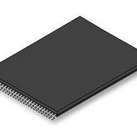
S29GL256P11TFI010 Spansion Inc., S29GL256P11TFI010 Datasheet - Page 63

S29GL256P11TFI010
Manufacturer Part Number
S29GL256P11TFI010
Description
Flash 3V 256Mb Mirrorbit highest address110ns
Manufacturer
Spansion Inc.
Specifications of S29GL256P11TFI010
Memory Type
NOR
Memory Size
256 Mbit
Access Time
110 ns
Data Bus Width
8 bit, 16 bit
Architecture
Uniform
Interface Type
Page-mode
Supply Voltage (max)
3.6 V
Supply Voltage (min)
2.7 V
Maximum Operating Current
50 mA
Mounting Style
SMD/SMT
Operating Temperature
+ 85 C
Package / Case
TSOP-56
Memory Configuration
128K X 16
Ic Interface Type
Parallel
Supply Voltage Range
2.7V To 3.6V
Memory Case Style
TSOP
No. Of Pins
56
Lead Free Status / RoHS Status
Lead free / RoHS Compliant
Lead Free Status / RoHS Status
Lead free / RoHS Compliant, Lead free / RoHS Compliant
Available stocks
Company
Part Number
Manufacturer
Quantity
Price
Company:
Part Number:
S29GL256P11TFI010
Manufacturer:
SPANSION
Quantity:
5 530
Company:
Part Number:
S29GL256P11TFI010
Manufacturer:
SPANSION
Quantity:
72
12. Appendix
12.1
Legend
X = Don’t care
RA = Address of the memory to be read.
RD = Data read from location RA during read operation.
PA = Address of the memory location to be programmed. Addresses latch on the falling edge of the WE# or CE# pulse, whichever happens later.
PD = Data to be programmed at location PA. Data latches on the rising edge of the WE# or CE# pulse, whichever happens first.
SA = Address of the sector to be verified (in autoselect mode) or erased. Address bits A
WBL = Write Buffer Location. The address must be within the same write buffer page as PA.
WC = Word Count is the number of write buffer locations to load minus 1.
Notes
1. See
2. All values are in hexadecimal.
3. All bus cycles are write cycles unless otherwise noted.
4. Data bits DQ15-DQ8 are don’t cares for unlock and command cycles.
5. Address bits A
6. No unlock or command cycles required when reading array data.
November 21, 2006 S29GL-P_00_A3
Read
Reset
CFI Query
Program
Write to Buffer
Program Buffer to Flash (Confirm)
Write-to-Buffer-Abort Reset
Chip Erase
Sector Erase
Erase Suspend/Program Suspend
Erase Resume/Program Resume
Secured Silicon Sector Entry
Secured Silicon Sector Exit
Manufacturer ID
Device ID
Sector Protect Verify
Secure Device Verify
Enter
Program
Sector Erase
Chip Erase
Reset
(6)
(7)
Table 7.1 on page 14
(12)
(15)
Command Definitions
Command (Notes)
(14)
(8)
MAX
(14)
(14)
:A16 are don’t cares for unlock and command cycles, unless SA or PA required. (A
This section contains information relating to software control or interfacing with the Flash device. For
additional information and assistance regarding software, see
the Spansion web site at www.spansion.com.
Writing specific address and data commands or sequences into the command register initiates device
operations. Tables
data values or writing them in the improper sequence can place the device in an unknown state. A reset
command is then required to return the device to reading array data.
(10)
D a t a
(11)
(18)
(13)
for description of bus operations.
(17)
(16)
Table 12.1 S29GL-P Memory Array Command Definitions, x16
S h e e t
12.1–12.4
1
1
4
4
4
4
1
4
3
1
3
3
2
2
2
2
6
6
1
1
3
4
Addr
XXX
XXX
XXX
XXX
XXX
XXX
XXX
555
555
555
555
555
555
555
555
555
555
555
555
RA
SA
55
( A d v a n c e
First
S29GL-P MirrorBit
define the valid register command sequences. Writing incorrect address and
Data
RD
AA
AA
AA
AA
AA
AA
AA
AA
AA
AA
AA
AA
F0
98
29
A0
80
80
90
B0
30
Addr
2AA
2AA
2AA
2AA
2AA
2AA
2AA
2AA
XXX
XXX
2AA
2AA
2AA
2AA
SA
PA
Second
I n f o r m a t i o n )
Data
PD
55
55
55
55
55
55
55
55
30
10
00
55
55
55
55
TM
Flash Family
max
Addr
–A16 uniquely select any sector.
555
555
555
555
555
555
555
555
555
555
555
SA
Third
Bus Cycles (Notes 1–5)
Data
A0
F0
90
90
90
90
25
20
80
80
88
90
Section 5.
MAX
[SA]X02
is the Highest Address pin.).
Addr
X00
X01
X03
555
555
SA
XX
PA
Fourth
For the latest information, explore
227E
Data
(10)
(11)
WC
PD
AA
AA
01
00
Addr
WBL
X0E
2AA
2AA
Fifth
Data
PD
(8)
55
55
Addr
WBL
X0F
555
SA
Sixth
Data
PD
(8)
10
30
61


