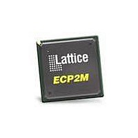
LFE2M35E-6FN484C Lattice, LFE2M35E-6FN484C Datasheet - Page 18

LFE2M35E-6FN484C
Manufacturer Part Number
LFE2M35E-6FN484C
Description
FPGA - Field Programmable Gate Array 34K LUTs SERDES MEM DSP 1.2V -6 Spd
Manufacturer
Lattice
Series
LatticeECP2Mr
Datasheet
1.LFE2-12SE-6FN256C.pdf
(389 pages)
Specifications of LFE2M35E-6FN484C
Number Of Macrocells
34000
Maximum Operating Frequency
357 MHz
Number Of Programmable I/os
303
Data Ram Size
2151424
Supply Voltage (max)
1.26 V
Maximum Operating Temperature
+ 85 C
Minimum Operating Temperature
0 C
Mounting Style
SMD/SMT
Supply Voltage (min)
1.14 V
Package / Case
FPBGA-484
No. Of Logic Blocks
34000
No. Of Macrocells
16000
No. Of Speed Grades
6
Total Ram Bits
2101Kbit
No. Of I/o's
303
Clock Management
DLL, PLL
I/o Supply Voltage
3.465V
Rohs Compliant
Yes
Lead Free Status / RoHS Status
Lead free / RoHS Compliant
Available stocks
Company
Part Number
Manufacturer
Quantity
Price
Company:
Part Number:
LFE2M35E-6FN484C
Manufacturer:
Lattice
Quantity:
135
Company:
Part Number:
LFE2M35E-6FN484C
Manufacturer:
LATTICE
Quantity:
168
Company:
Part Number:
LFE2M35E-6FN484C
Manufacturer:
Lattice Semiconductor Corporation
Quantity:
10 000
Company:
Part Number:
LFE2M35E-6FN484C-5I
Manufacturer:
LATTICE
Quantity:
1
- Current page: 18 of 389
- Download datasheet (5Mb)
Architecture
Lattice Semiconductor
LatticeECP2/M Family Data Sheet
Primary Clock Routing
The clock routing structure in LatticeECP2/M devices consists of a network of eight primary clock lines (CLK0
through CLK7) per quadrant. The primary clocks of each quadrant are generated from muxes located in the center
of the device. All the clock sources are connected to these muxes. Figure 2-13 shows the clock routing for one
quadrant. Each quadrant mux is identical. If desired, any clock can be routed globally
Figure 2-13. Per Quadrant Primary Clock Selection
Primary Clock Sources: PLLs + DLLs + CLKDIVs + PIOs + Routing
35:1
35:1
35:1
35:1
35:1
35:1
32:1
32:1
32:1
32:1
DCS
DCS
CLK0
CLK1
CLK2
CLK3
CLK4
CLK5
CLK6
CLK7
8 Primary Clocks (CLK0 to CLK7) per Quadrant
Dynamic Clock Select (DCS)
The DCS is a smart multiplexer function available in the primary clock routing. It switches between two independent
input clock sources without any glitches or runt pulses. This is achieved regardless of when the select signal is tog-
gled. There are two DCS blocks per quadrant; in total, there are eight DCS blocks per device. The inputs to the
DCS block come from the center muxes. The output of the DCS is connected to primary clocks CLK6 and CLK7
(see Figure 2-13).
Figure 2-14 shows the timing waveforms of the default DCS operating mode. The DCS block can be programmed
to other modes. For more information about the DCS, please see the list of additional technical documentation at
the end of this data sheet.
Figure 2-14. DCS Waveforms
CLK0
CLK1
SEL
DCSOUT
Secondary Clock/Control Routing
Secondary clocks in the LatticeECP2 devices are region-based resources. The benefit of region-based resources
is the relatively low injection delay and skew within the region, as compared to primary clocks. EBR/DSP rows and
a special vertical routing channel bound the secondary clock regions. This special vertical routing channel aligns
with either the left edge of the center DSP block in the DSP row or the center of the DSP row. Figure 2-15 shows
2-15
Related parts for LFE2M35E-6FN484C
Image
Part Number
Description
Manufacturer
Datasheet
Request
R

Part Number:
Description:
FPGA - Field Programmable Gate Array 34K LUTs SERDES MEM DSP 1.2V -6 Spd I
Manufacturer:
Lattice

Part Number:
Description:
FPGA - Field Programmable Gate Array 34K LUTs SERDES MEM DSP 1.2V -5 Spd
Manufacturer:
Lattice
Datasheet:
Part Number:
Description:
IC, LATTICEECP2M FPGA, 420MHZ, FPBGA-672
Manufacturer:
LATTICE SEMICONDUCTOR
Datasheet:
Part Number:
Description:
IC, LATTICEECP2M FPGA, 420MHZ, FPBGA-256
Manufacturer:
LATTICE SEMICONDUCTOR
Datasheet:
Part Number:
Description:
FPGA LatticeECP2M Family 34000 Cells 90nm (CMOS) Technology 1.2V 484-Pin FBGA
Manufacturer:
LATTICE SEMICONDUCTOR
Datasheet:
Part Number:
Description:
FPGA LatticeECP2M Family 34000 Cells 90nm (CMOS) Technology 1.2V 484-Pin FBGA
Manufacturer:
LATTICE SEMICONDUCTOR
Datasheet:
Part Number:
Description:
FPGA LatticeECP2M Family 34000 Cells 90nm (CMOS) Technology 1.2V 256-Pin FBGA
Manufacturer:
LATTICE SEMICONDUCTOR
Datasheet:
Part Number:
Description:
FPGA LatticeECP2M Family 34000 Cells 90nm (CMOS) Technology 1.2V 484-Pin FBGA
Manufacturer:
LATTICE SEMICONDUCTOR
Datasheet:
Part Number:
Description:
FPGA LatticeECP2M Family 34000 Cells 90nm (CMOS) Technology 1.2V 484-Pin FBGA
Manufacturer:
LATTICE SEMICONDUCTOR
Datasheet:

Part Number:
Description:
IC FPGA 35KLUTS 410I/O 672-BGA
Manufacturer:
Lattice
Datasheet:

Part Number:
Description:
IC FPGA 35KLUTS 140I/O 256-BGA
Manufacturer:
Lattice
Datasheet:

Part Number:
Description:
IC FPGA 35KLUTS 140I/O 256-BGA
Manufacturer:
Lattice
Datasheet:

Part Number:
Description:
IC FPGA 35KLUTS 140I/O 256-BGA
Manufacturer:
Lattice
Datasheet:

Part Number:
Description:
IC FPGA 35KLUTS 140I/O 256-BGA
Manufacturer:
Lattice
Datasheet:

Part Number:
Description:
IC FPGA 35KLUTS 303I/O 484-BGA
Manufacturer:
Lattice
Datasheet:


