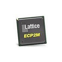
LFE2M35E-6FN484C Lattice, LFE2M35E-6FN484C Datasheet - Page 42

LFE2M35E-6FN484C
Manufacturer Part Number
LFE2M35E-6FN484C
Description
FPGA - Field Programmable Gate Array 34K LUTs SERDES MEM DSP 1.2V -6 Spd
Manufacturer
Lattice
Series
LatticeECP2Mr
Datasheet
1.LFE2-12SE-6FN256C.pdf
(389 pages)
Specifications of LFE2M35E-6FN484C
Number Of Macrocells
34000
Maximum Operating Frequency
357 MHz
Number Of Programmable I/os
303
Data Ram Size
2151424
Supply Voltage (max)
1.26 V
Maximum Operating Temperature
+ 85 C
Minimum Operating Temperature
0 C
Mounting Style
SMD/SMT
Supply Voltage (min)
1.14 V
Package / Case
FPBGA-484
No. Of Logic Blocks
34000
No. Of Macrocells
16000
No. Of Speed Grades
6
Total Ram Bits
2101Kbit
No. Of I/o's
303
Clock Management
DLL, PLL
I/o Supply Voltage
3.465V
Rohs Compliant
Yes
Lead Free Status / RoHS Status
Lead free / RoHS Compliant
Available stocks
Company
Part Number
Manufacturer
Quantity
Price
Company:
Part Number:
LFE2M35E-6FN484C
Manufacturer:
Lattice
Quantity:
135
Company:
Part Number:
LFE2M35E-6FN484C
Manufacturer:
LATTICE
Quantity:
168
Company:
Part Number:
LFE2M35E-6FN484C
Manufacturer:
Lattice Semiconductor Corporation
Quantity:
10 000
Company:
Part Number:
LFE2M35E-6FN484C-5I
Manufacturer:
LATTICE
Quantity:
1
- Current page: 42 of 389
- Download datasheet (5Mb)
Lattice Semiconductor
Figure 2-36. DQS Local Bus
Polarity Control Logic
In a typical DDR Memory interface design, the phase relationship between the incoming delayed DQS strobe and
the internal system clock (during the READ cycle) is unknown.
The LatticeECP2/M family contains dedicated circuits to transfer data between these domains. To prevent set-up
and hold violations, at the domain transfer between DQS (delayed) and the system clock, a clock polarity selector
is used. This changes the edge on which the data is registered in the synchronizing registers in the input register
block. This requires evaluation at the start of each READ cycle for the correct clock polarity.
Prior to the READ operation in DDR memories, DQS is in tristate (pulled by termination). The DDR memory device
drives DQS low at the start of the preamble state. A dedicated circuit detects the first DQS rising edge after the pre-
amble state. This signal is used to control the polarity of the clock to the synchronizing registers.
*DQSXFERDEL shifts ECLK1 by 90% and is not associated with a particular PIO.
DQSXFER
DQS
DQS
DCNTL[6:0]
ECLK1
DQSXFER
DCNTL[6:0]
CLK1
GSR
DQS
CEI
2-39
DQSXFERDEL*
Polarity Control
DQSDEL
Logic
PIO
PIO
To DDR
Register Block
Register Block
Reg.
Output
Input
Calibration bus
To Sync
LatticeECP2/M Family Data Sheet
from DLL
Reg.
Buffer
Buffer
sysIO
sysIO
DI
DI
Strobe
Datain
DDR
DQS
PAD
PAD
Architecture
Related parts for LFE2M35E-6FN484C
Image
Part Number
Description
Manufacturer
Datasheet
Request
R

Part Number:
Description:
FPGA - Field Programmable Gate Array 34K LUTs SERDES MEM DSP 1.2V -6 Spd I
Manufacturer:
Lattice

Part Number:
Description:
FPGA - Field Programmable Gate Array 34K LUTs SERDES MEM DSP 1.2V -5 Spd
Manufacturer:
Lattice
Datasheet:
Part Number:
Description:
IC, LATTICEECP2M FPGA, 420MHZ, FPBGA-672
Manufacturer:
LATTICE SEMICONDUCTOR
Datasheet:
Part Number:
Description:
IC, LATTICEECP2M FPGA, 420MHZ, FPBGA-256
Manufacturer:
LATTICE SEMICONDUCTOR
Datasheet:
Part Number:
Description:
FPGA LatticeECP2M Family 34000 Cells 90nm (CMOS) Technology 1.2V 484-Pin FBGA
Manufacturer:
LATTICE SEMICONDUCTOR
Datasheet:
Part Number:
Description:
FPGA LatticeECP2M Family 34000 Cells 90nm (CMOS) Technology 1.2V 484-Pin FBGA
Manufacturer:
LATTICE SEMICONDUCTOR
Datasheet:
Part Number:
Description:
FPGA LatticeECP2M Family 34000 Cells 90nm (CMOS) Technology 1.2V 256-Pin FBGA
Manufacturer:
LATTICE SEMICONDUCTOR
Datasheet:
Part Number:
Description:
FPGA LatticeECP2M Family 34000 Cells 90nm (CMOS) Technology 1.2V 484-Pin FBGA
Manufacturer:
LATTICE SEMICONDUCTOR
Datasheet:
Part Number:
Description:
FPGA LatticeECP2M Family 34000 Cells 90nm (CMOS) Technology 1.2V 484-Pin FBGA
Manufacturer:
LATTICE SEMICONDUCTOR
Datasheet:

Part Number:
Description:
IC FPGA 35KLUTS 410I/O 672-BGA
Manufacturer:
Lattice
Datasheet:

Part Number:
Description:
IC FPGA 35KLUTS 140I/O 256-BGA
Manufacturer:
Lattice
Datasheet:

Part Number:
Description:
IC FPGA 35KLUTS 140I/O 256-BGA
Manufacturer:
Lattice
Datasheet:

Part Number:
Description:
IC FPGA 35KLUTS 140I/O 256-BGA
Manufacturer:
Lattice
Datasheet:

Part Number:
Description:
IC FPGA 35KLUTS 140I/O 256-BGA
Manufacturer:
Lattice
Datasheet:

Part Number:
Description:
IC FPGA 35KLUTS 303I/O 484-BGA
Manufacturer:
Lattice
Datasheet:


