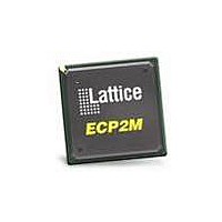
LFE2M35E-6FN484C Lattice, LFE2M35E-6FN484C Datasheet - Page 20

LFE2M35E-6FN484C
Manufacturer Part Number
LFE2M35E-6FN484C
Description
FPGA - Field Programmable Gate Array 34K LUTs SERDES MEM DSP 1.2V -6 Spd
Manufacturer
Lattice
Series
LatticeECP2Mr
Datasheet
1.LFE2-12SE-6FN256C.pdf
(389 pages)
Specifications of LFE2M35E-6FN484C
Number Of Macrocells
34000
Maximum Operating Frequency
357 MHz
Number Of Programmable I/os
303
Data Ram Size
2151424
Supply Voltage (max)
1.26 V
Maximum Operating Temperature
+ 85 C
Minimum Operating Temperature
0 C
Mounting Style
SMD/SMT
Supply Voltage (min)
1.14 V
Package / Case
FPBGA-484
No. Of Logic Blocks
34000
No. Of Macrocells
16000
No. Of Speed Grades
6
Total Ram Bits
2101Kbit
No. Of I/o's
303
Clock Management
DLL, PLL
I/o Supply Voltage
3.465V
Rohs Compliant
Yes
Lead Free Status / RoHS Status
Lead free / RoHS Compliant
Available stocks
Company
Part Number
Manufacturer
Quantity
Price
Company:
Part Number:
LFE2M35E-6FN484C
Manufacturer:
Lattice
Quantity:
135
Company:
Part Number:
LFE2M35E-6FN484C
Manufacturer:
LATTICE
Quantity:
168
Company:
Part Number:
LFE2M35E-6FN484C
Manufacturer:
Lattice Semiconductor Corporation
Quantity:
10 000
Company:
Part Number:
LFE2M35E-6FN484C-5I
Manufacturer:
LATTICE
Quantity:
1
- Current page: 20 of 389
- Download datasheet (5Mb)
Lattice Semiconductor
Figure 2-16. Secondary Clock Selection
Slice Clock Selection
Figure 2-17 shows the clock selections and Figure 2-18 shows the control selections for Slice0 through Slice2. All
the primary clocks and the four secondary clocks are routed to this clock selection mux. Other signals can be used
as a clock input to the slices via routing. Slice controls are generated from the secondary clocks or other signals
connected via routing.
If none of the signals are selected for both clock and control then the default value of the mux output is 1. Slice 3
does not have any registers; therefore it does not have the clock or control muxes.
Figure 2-17. Slice0 through Slice2 Clock Selection
4 Secondary Clocks/CE/LSR (SC0 to SC3) per Region
SC0
24:1
Secondary Clock
Primary Clock
SC1
24:1
Clock/Control
Routing
Secondary Clock Feedlines: 8 PIOs + 16 Routing
SC2
Vcc
24:1
SC3
12
24:1
8
4
1
4 High Fan-out Data Signals (SC4 to SC7) per Region
2-17
SC4
24:1
25:1
SC5
High Fan-out Data
24:1
LatticeECP2/M Family Data Sheet
Clock to Slice
SC6
24:1
SC7
24:1
Architecture
Related parts for LFE2M35E-6FN484C
Image
Part Number
Description
Manufacturer
Datasheet
Request
R

Part Number:
Description:
FPGA - Field Programmable Gate Array 34K LUTs SERDES MEM DSP 1.2V -6 Spd I
Manufacturer:
Lattice

Part Number:
Description:
FPGA - Field Programmable Gate Array 34K LUTs SERDES MEM DSP 1.2V -5 Spd
Manufacturer:
Lattice
Datasheet:
Part Number:
Description:
IC, LATTICEECP2M FPGA, 420MHZ, FPBGA-672
Manufacturer:
LATTICE SEMICONDUCTOR
Datasheet:
Part Number:
Description:
IC, LATTICEECP2M FPGA, 420MHZ, FPBGA-256
Manufacturer:
LATTICE SEMICONDUCTOR
Datasheet:
Part Number:
Description:
FPGA LatticeECP2M Family 34000 Cells 90nm (CMOS) Technology 1.2V 484-Pin FBGA
Manufacturer:
LATTICE SEMICONDUCTOR
Datasheet:
Part Number:
Description:
FPGA LatticeECP2M Family 34000 Cells 90nm (CMOS) Technology 1.2V 484-Pin FBGA
Manufacturer:
LATTICE SEMICONDUCTOR
Datasheet:
Part Number:
Description:
FPGA LatticeECP2M Family 34000 Cells 90nm (CMOS) Technology 1.2V 256-Pin FBGA
Manufacturer:
LATTICE SEMICONDUCTOR
Datasheet:
Part Number:
Description:
FPGA LatticeECP2M Family 34000 Cells 90nm (CMOS) Technology 1.2V 484-Pin FBGA
Manufacturer:
LATTICE SEMICONDUCTOR
Datasheet:
Part Number:
Description:
FPGA LatticeECP2M Family 34000 Cells 90nm (CMOS) Technology 1.2V 484-Pin FBGA
Manufacturer:
LATTICE SEMICONDUCTOR
Datasheet:

Part Number:
Description:
IC FPGA 35KLUTS 410I/O 672-BGA
Manufacturer:
Lattice
Datasheet:

Part Number:
Description:
IC FPGA 35KLUTS 140I/O 256-BGA
Manufacturer:
Lattice
Datasheet:

Part Number:
Description:
IC FPGA 35KLUTS 140I/O 256-BGA
Manufacturer:
Lattice
Datasheet:

Part Number:
Description:
IC FPGA 35KLUTS 140I/O 256-BGA
Manufacturer:
Lattice
Datasheet:

Part Number:
Description:
IC FPGA 35KLUTS 140I/O 256-BGA
Manufacturer:
Lattice
Datasheet:

Part Number:
Description:
IC FPGA 35KLUTS 303I/O 484-BGA
Manufacturer:
Lattice
Datasheet:


