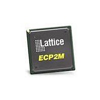
LFE2M35E-6FN484C Lattice, LFE2M35E-6FN484C Datasheet - Page 94

LFE2M35E-6FN484C
Manufacturer Part Number
LFE2M35E-6FN484C
Description
FPGA - Field Programmable Gate Array 34K LUTs SERDES MEM DSP 1.2V -6 Spd
Manufacturer
Lattice
Series
LatticeECP2Mr
Datasheet
1.LFE2-12SE-6FN256C.pdf
(389 pages)
Specifications of LFE2M35E-6FN484C
Number Of Macrocells
34000
Maximum Operating Frequency
357 MHz
Number Of Programmable I/os
303
Data Ram Size
2151424
Supply Voltage (max)
1.26 V
Maximum Operating Temperature
+ 85 C
Minimum Operating Temperature
0 C
Mounting Style
SMD/SMT
Supply Voltage (min)
1.14 V
Package / Case
FPBGA-484
No. Of Logic Blocks
34000
No. Of Macrocells
16000
No. Of Speed Grades
6
Total Ram Bits
2101Kbit
No. Of I/o's
303
Clock Management
DLL, PLL
I/o Supply Voltage
3.465V
Rohs Compliant
Yes
Lead Free Status / RoHS Status
Lead free / RoHS Compliant
Available stocks
Company
Part Number
Manufacturer
Quantity
Price
Company:
Part Number:
LFE2M35E-6FN484C
Manufacturer:
Lattice
Quantity:
135
Company:
Part Number:
LFE2M35E-6FN484C
Manufacturer:
LATTICE
Quantity:
168
Company:
Part Number:
LFE2M35E-6FN484C
Manufacturer:
Lattice Semiconductor Corporation
Quantity:
10 000
Company:
Part Number:
LFE2M35E-6FN484C-5I
Manufacturer:
LATTICE
Quantity:
1
- Current page: 94 of 389
- Download datasheet (5Mb)
Lattice Semiconductor
Table 3-13. Periodic Receiver Jitter Tolerance Specification
Periodic
1. Values are measured with PRBS 2
2. Jitter specification is limited by measurement equipment capability.
Description
3.125 Gbps 600 mV differential eye
2.5 Gbps
1.25 Gbps
250 Mbps
Frequency
2
600 mV differential eye
600 mV differential eye
600 mV differential eye
7
-1, all channels operating.
Condition
3-42
Min.
—
—
—
—
1
DC and Switching Characteristics
LatticeECP2/M Family Data Sheet
Typ.
—
—
—
—
Max.
0.22
0.08
0.20
0.20
UI, p-p
UI, p-p
UI, p-p
UI, p-p
Units
Related parts for LFE2M35E-6FN484C
Image
Part Number
Description
Manufacturer
Datasheet
Request
R

Part Number:
Description:
FPGA - Field Programmable Gate Array 34K LUTs SERDES MEM DSP 1.2V -6 Spd I
Manufacturer:
Lattice

Part Number:
Description:
FPGA - Field Programmable Gate Array 34K LUTs SERDES MEM DSP 1.2V -5 Spd
Manufacturer:
Lattice
Datasheet:
Part Number:
Description:
IC, LATTICEECP2M FPGA, 420MHZ, FPBGA-672
Manufacturer:
LATTICE SEMICONDUCTOR
Datasheet:
Part Number:
Description:
IC, LATTICEECP2M FPGA, 420MHZ, FPBGA-256
Manufacturer:
LATTICE SEMICONDUCTOR
Datasheet:
Part Number:
Description:
FPGA LatticeECP2M Family 34000 Cells 90nm (CMOS) Technology 1.2V 484-Pin FBGA
Manufacturer:
LATTICE SEMICONDUCTOR
Datasheet:
Part Number:
Description:
FPGA LatticeECP2M Family 34000 Cells 90nm (CMOS) Technology 1.2V 484-Pin FBGA
Manufacturer:
LATTICE SEMICONDUCTOR
Datasheet:
Part Number:
Description:
FPGA LatticeECP2M Family 34000 Cells 90nm (CMOS) Technology 1.2V 256-Pin FBGA
Manufacturer:
LATTICE SEMICONDUCTOR
Datasheet:
Part Number:
Description:
FPGA LatticeECP2M Family 34000 Cells 90nm (CMOS) Technology 1.2V 484-Pin FBGA
Manufacturer:
LATTICE SEMICONDUCTOR
Datasheet:
Part Number:
Description:
FPGA LatticeECP2M Family 34000 Cells 90nm (CMOS) Technology 1.2V 484-Pin FBGA
Manufacturer:
LATTICE SEMICONDUCTOR
Datasheet:

Part Number:
Description:
IC FPGA 35KLUTS 410I/O 672-BGA
Manufacturer:
Lattice
Datasheet:

Part Number:
Description:
IC FPGA 35KLUTS 140I/O 256-BGA
Manufacturer:
Lattice
Datasheet:

Part Number:
Description:
IC FPGA 35KLUTS 140I/O 256-BGA
Manufacturer:
Lattice
Datasheet:

Part Number:
Description:
IC FPGA 35KLUTS 140I/O 256-BGA
Manufacturer:
Lattice
Datasheet:

Part Number:
Description:
IC FPGA 35KLUTS 140I/O 256-BGA
Manufacturer:
Lattice
Datasheet:

Part Number:
Description:
IC FPGA 35KLUTS 303I/O 484-BGA
Manufacturer:
Lattice
Datasheet:


