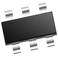
MCP4706A3T-E/CH Microchip Technology, MCP4706A3T-E/CH Datasheet - Page 35

MCP4706A3T-E/CH
Manufacturer Part Number
MCP4706A3T-E/CH
Description
Single, 8-bit NV DAC With Ext Vref And I2C Interface 6 SOT-23 T/R
Manufacturer
Microchip Technology
Series
-r
Datasheet
1.MCP4706A0T-ECH.pdf
(86 pages)
Specifications of MCP4706A3T-E/CH
Number Of Converters
1
Conversion Rate
1
Resolution
8 bit
Interface Type
I2C
Settling Time
6 us
Supply Voltage (max)
5.5 V
Supply Voltage (min)
2.7 V
Maximum Operating Temperature
+ 125 C
Mounting Style
SMD/SMT
Package / Case
SOT-23-6
Maximum Power Dissipation
452 mW
Minimum Operating Temperature
- 40 C
Supply Current
210 uA
Number Of Bits
8
Data Interface
EEPROM, I²C, Serial
Voltage Supply Source
Single Supply
Power Dissipation (max)
452mW
Operating Temperature
-40°C ~ 125°C
Mounting Type
Surface Mount
Number Of Outputs And Type
*
Lead Free Status / Rohs Status
Details
4.0
The MCP4706, MCP4716, and MCP4726 devices are
single channel voltage output 8-bit, 10-bit, and 12-bit
DAC devices with nonvolatile memory (EEPROM) and
an I
MCP47X6.
The devices use a resistor ladder architecture. The
resistor ladder DAC is driven from a software
selectable voltage reference source. The source can
be either the device’s internal V
pin voltage.
The DAC output is buffered with a low power and
precision output amplifier (op amp). This output
amplifier provides a rail-to-rail output with low offset
voltage and low noise. The gain of the output buffer is
software configurable.
This device also has user programmable nonvolatile
memory (EEPROM), which allows the user to save the
desired POR/BOR value of the DAC register and
device configuration bits.
The devices use a two-wire I
interface and operate with a single supply voltage from
2.7V to 5.5V.
FIGURE 4-1:
© 2011 Microchip Technology Inc.
V
DD(MIN
2
C serial interface. This family will be referred to as
V
V
POR
RAM
GENERAL DESCRIPTION
)
Device in
unknown
state
POR reset forced active
Volatile memory
retains data value
Power-On-Reset Operation.
Device in
POR state
T
(60 µs max.)
2
PORD
C serial communication
DD
or the external V
POR starts Reset Delay Timer.
When timer times out, I
can operate (if V
EEPROM data latched into volatile
configuration bits and DAC register.
POR status bit is set (“1”)
REF
Normal Operation
DD
>= V
2
C interface
DD(MIN)
4.1
The internal Power-On-Reset (POR) / Brown-Out
Reset (BOR) circuit monitors the power supply voltage
(V
device start-up at system power-up and power-down
events. V
always lower than the POR trip point voltage.
POR occurs as the voltage is rising (typically from 0V),
while BOR occurs as the voltage is falling (typically
from V
When the rising V
point, the following occurs:
• Nonvolatile DAC Register value latched into
• Nonvolatile configuration bit values latched into
• POR status bit is set (“1”)
• The reset delay timer starts; when timer times out
The analog output (V
the state of the volatile configuration bits and the DAC
Register. This is called a POR reset (event).
When the falling V
point, the following occurs:
• Device is forced into a power down state
• Volatile DAC Register is forced to 000h
• Volatile configuration bits V
Figure 4-1
power-down events under typical conditions.
MCP4706/4716/4726
DD
volatile DAC Register
volatile configuration bits
(t
(PD1:PD0 = ‘11’). Analog circuitry is turned off.
forced to ‘0’
PORD
) during operation. This circuit ensures correct
)
DD(MIN)
), the I
Power-On-Reset / Brown Out
Reset (POR/BOR)
RAM
illustrates the conditions for power-up and
or higher).
is the RAM retention voltage and is
2
C interface is operational.
Below
minimum
operating
voltage
DD
DD
OUT
voltage crosses the V
voltage crosses the V
BOR reset,
volatile DAC Register = 000h
volatile VREF1:VREF0 = 00
volatile G = 0
volatile PD1:PD0 = 11
) state will be determined by
Volatile memory
becomes corrupted
Device
in power
down
state
REF1
, V
REF0
DS22272A-page 35
Device in
unknown
state
and G are
V
POR
POR
BOR
trip
trip


