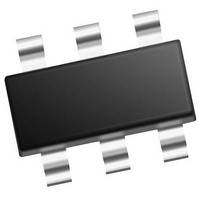
MCP4706A3T-E/CH Microchip Technology, MCP4706A3T-E/CH Datasheet - Page 40

MCP4706A3T-E/CH
Manufacturer Part Number
MCP4706A3T-E/CH
Description
Single, 8-bit NV DAC With Ext Vref And I2C Interface 6 SOT-23 T/R
Manufacturer
Microchip Technology
Series
-r
Datasheet
1.MCP4706A0T-ECH.pdf
(86 pages)
Specifications of MCP4706A3T-E/CH
Number Of Converters
1
Conversion Rate
1
Resolution
8 bit
Interface Type
I2C
Settling Time
6 us
Supply Voltage (max)
5.5 V
Supply Voltage (min)
2.7 V
Maximum Operating Temperature
+ 125 C
Mounting Style
SMD/SMT
Package / Case
SOT-23-6
Maximum Power Dissipation
452 mW
Minimum Operating Temperature
- 40 C
Supply Current
210 uA
Number Of Bits
8
Data Interface
EEPROM, I²C, Serial
Voltage Supply Source
Single Supply
Power Dissipation (max)
452mW
Operating Temperature
-40°C ~ 125°C
Mounting Type
Surface Mount
Number Of Outputs And Type
*
Lead Free Status / Rohs Status
Details
MCP4706/4716/4726
4.6
Device Resets can be grouped into two types. Resets
due to change in voltage (POR/BOR Reset), and resets
caused
microcontroller).
After a device reset, and when V
device memory may be written or read.
4.6.1
The POR and BOR trip points are at the same voltage,
and is determined if the V
(see
the reset is a POR or BOR reset.
POR Reset (V
On a POR Reset, the nonvolatile memory values (DAC
Register and Configuration bits) are latched into the
volatile memory. This configures the analog output
(V
this delay time, the I
commands.
BOR Reset (V
On a BOR Reset, the device is forced into a power
down state. The volatile PD1:PD0 bits forced to ‘11’ and
all other volatile memory forced to ‘0’. The I
will not accept commands.
4.6.2
When the MCP47X6 is in the valid operating voltage,
the I
event. This is similar to the POR reset, except that the
reset delay timer is not started.
In the case where the I
to be responsive, the technique shown in
Software I2C Interface Reset Sequence
to force the I
FIGURE 4-6:
DS22272A-page 40
OUT
V
V
Note 1: The D
2
REF1
REF1
Figure
C General Call Reset command will force a reset
) circuitry. Also a reset delay timer starts. During
2: Status bits are read only
Device Resets
by
V
V
POR/BOR RESET OPERATION
RESET COMMANDS
and the MCP4726: D
4-1). What occurs is different depending if
2
REF0
REF0
C interface to be reset.
the
Config Bits
DD
MAX
DD
PD1
PD1
system
Rising)
Falling)
value depends on the device. For the MCP4706: D
DAC Memory and POR Interaction.
2
C Interface bus does not seem
2
C interface will not accept
DD
PD0
PD0
voltage is rising or falling
master
MAX
DD
G
G
= D
≥ V
(such
11
Section 8.9,
can be used
DD(MIN)
2
.
C interface
RDY/BSY
as
Status Bits
, the
a
POR
(2)
4.7
The MCP47X6 devices have both volatile and
nonvolatile (EEPROM) memory.
volatile and nonvolatile memory and their interaction
due to a POR event.
There are five configuration bits in both the volatile and
nonvolatile memory, the DAC registers in both the
volatile and nonvolatile memory, and two volatile status
bits. The DAC registers (volatile and nonvolatile) will be
either 12-bits (MCP4726), 10-bits (MCP4716), or 8-bits
(MCP4706) wide.
When the device is first powered up, it automatically
uploads the EEPROM memory values to the volatile
memory. The volatile memory determines the analog
output (V
up, the user can update the device memory.
The I
written. Refer to
and
more details on the reading and writing the device’s
memory.
When the nonvolatile memory is written (using the I
Write All Memory command), the volatile memory is
written with the same values. The device starts writing
the EEPROM cell at the acknowledge pulse of the
EEPROM write command.
Table 4-3
Table 4-4
configuration bits, and
default value of a POR/BOR event for the device
configuration bits.
There are two Status bits. These are only in volatile
memory and give indication on the status of the device.
The POR bit indicates if the device V
below the POR trip point. During normal operation, this
bit should be ‘1’. The RDY/BSY bit indicates if an
EEPROM write cycle is in progress. While the RDY/
BSY bit is low (during the EEPROM writing), all
commands are ignored, except for the Read Command
command.
D
D
Section 6.0 “MCP47X6 I2C Commands”
2
MAX
MAX
C interface is how this memory is read and
DAC Registers, Configuration
Bits, and Status Bits
OUT
shows the operation of the device status bits,
MAX
DAC Register Value
shows the
) pin voltage. After the device is powered
= D
7
Section 5.0 “I
, MCP4716: D
© 2011 Microchip Technology Inc.
Table 4-5
operation
D
D
1
1
(1)
2
Figure 4-6
MAX
C Serial Interface”
D
D
shows the factory
0
0
= D
of
DD
N.V. Memory
POR Event
Vol. Memory
9
,
the
is above or
shows the
device
for
2
C


