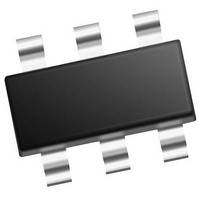
MCP4706A3T-E/CH Microchip Technology, MCP4706A3T-E/CH Datasheet - Page 43

MCP4706A3T-E/CH
Manufacturer Part Number
MCP4706A3T-E/CH
Description
Single, 8-bit NV DAC With Ext Vref And I2C Interface 6 SOT-23 T/R
Manufacturer
Microchip Technology
Series
-r
Datasheet
1.MCP4706A0T-ECH.pdf
(86 pages)
Specifications of MCP4706A3T-E/CH
Number Of Converters
1
Conversion Rate
1
Resolution
8 bit
Interface Type
I2C
Settling Time
6 us
Supply Voltage (max)
5.5 V
Supply Voltage (min)
2.7 V
Maximum Operating Temperature
+ 125 C
Mounting Style
SMD/SMT
Package / Case
SOT-23-6
Maximum Power Dissipation
452 mW
Minimum Operating Temperature
- 40 C
Supply Current
210 uA
Number Of Bits
8
Data Interface
EEPROM, I²C, Serial
Voltage Supply Source
Single Supply
Power Dissipation (max)
452mW
Operating Temperature
-40°C ~ 125°C
Mounting Type
Surface Mount
Number Of Outputs And Type
*
Lead Free Status / Rohs Status
Details
5.0
The MCP47X6 devices support the I
The MCP47X6 I
(does not generate the serial clock).
5.1
This I
shows a typical I
The I
rates. These are referred to as standard, fast or high
speed modes. The MCP47X6 supports these three
modes. The bit rates of these modes are:
• Standard Mode: bit rates up to 100 kbit/s
• Fast Mode: bit rates up to 400 kbit/s
• High Speed Mode (HS mode): bit rates up to
A device that sends data onto the bus is defined as
transmitter, and a device receiving data as receiver.
The bus has to be controlled by a master device which
generates the serial clock (SCL), controls the bus
access and generates the START and STOP
conditions. The MCP47X6 device works as slave. Both
master and slave can operate as transmitter or
receiver, but the master device determines which mode
is activated. Communication is initiated by the master
(microcontroller) which sends the START bit, followed
by the slave address byte. The first byte transmitted is
always the slave address byte, which contains the
device code, the address bits, and the R/W bit.
FIGURE 5-1:
The I
lengths, timings, etc. of a frame. The frame content
defines the behavior of the device. For details on the
frame content (commands/data) refer to Section 6.0.
Refer to the NXP I
I
© 2011 Microchip Technology Inc.
2
C specifications.
Typical I
Controller
3.4 Mbit/s
Host
2
2
2
C serial protocol only defines the field types, field
C interface specifies different communication bit
C interface is a two-wire interface.
SCL
SDA
I
Overview
2
2
C SERIAL INTERFACE
C Interface Connections
2
2
C’s module operates in Slave mode
C Interface connection.
2
C document for more details on the
Typical I
2
C Interface.
2
C serial protocol.
SCL
SDA
MCP4XXX
Figure 5-1
5.2
The I
are:
• SDA (Serial Data)
• SCL (Serial Clock)
5.2.1
The Serial Data (SDA) signal is the data signal of the
device. The value on this pin is latched on the rising
edge of the SCL signal when the signal is an input.
With the exception of the START and STOP conditions,
the high or low state of the SDA pin can only change
when the clock signal on the SCL pin is low. During the
high period of the clock, the SDA pin’s value (high or
low) must be stable. Changes in the SDA pin’s value
while the SCL pin is HIGH will be interpreted as a
START or a STOP condition.
5.2.2
The Serial Clock (SCL) signal is the clock signal of the
device. The rising edge of the SCL signal latches the
value on the SDA pin.
The MCP47X6 will not stretch the clock signal (SCL)
since memory read access occurs fast enough.
Depending on the clock rate mode, the interface will
display different characteristics.
MCP4706/4716/4726
2
C interface uses up to two pins (signals). These
Signal Descriptions
SERIAL DATA (SDA)
SERIAL CLOCK (SCL)
DS22272A-page 43


