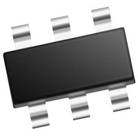
MCP4706A3T-E/CH Microchip Technology, MCP4706A3T-E/CH Datasheet - Page 67

MCP4706A3T-E/CH
Manufacturer Part Number
MCP4706A3T-E/CH
Description
Single, 8-bit NV DAC With Ext Vref And I2C Interface 6 SOT-23 T/R
Manufacturer
Microchip Technology
Series
-r
Datasheet
1.MCP4706A0T-ECH.pdf
(86 pages)
Specifications of MCP4706A3T-E/CH
Number Of Converters
1
Conversion Rate
1
Resolution
8 bit
Interface Type
I2C
Settling Time
6 us
Supply Voltage (max)
5.5 V
Supply Voltage (min)
2.7 V
Maximum Operating Temperature
+ 125 C
Mounting Style
SMD/SMT
Package / Case
SOT-23-6
Maximum Power Dissipation
452 mW
Minimum Operating Temperature
- 40 C
Supply Current
210 uA
Number Of Bits
8
Data Interface
EEPROM, I²C, Serial
Voltage Supply Source
Single Supply
Power Dissipation (max)
452mW
Operating Temperature
-40°C ~ 125°C
Mounting Type
Surface Mount
Number Of Outputs And Type
*
Lead Free Status / Rohs Status
Details
8.5
In some applications, precision digital control of the
output range is desirable.
to use the DAC devices to achieve this in a bipolar or
single-supply application.
This circuit is typically used for linearizing a sensor
whose slope and offset varies.
The equation to design a bipolar “window” DAC would
be utilized if R
8.5.1
An output step size of 1 mV, with an output range of
±2.05V, is desired for a particular application.
Step 1: Calculate the range: +2.05V – (-2.05V) = 4.1V.
Step 2: Calculate the resolution needed:
Step 3: The amplifier gain (R
The equation can be simplified to:
Step 4: Next, solve for R
Figure 8-6
© 2011 Microchip Technology Inc.
If R
4.1V/1 mV = 4100
Since 2
full-scale V
desired minimum output to achieve bipolar
operation. Since any gain can be realized by
choosing resistor values (R
must be selected first. If a V
solve for the amplifier’s gain by setting the DAC to
0, knowing that the output needs to be -2.05V.
4096, knowing that the output needs to be +2.05V.
1
= 20 kΩ and R
----------------------- -
(
R
Selectable Gain and Offset Bipolar
Voltage Output
3
R
(C1 = 0.1uF)
+
–
-------- -
BIPOLAR DAC EXAMPLE USING
MCP4726
If R
12
R
4
R
R
1
3
2
= 4096, 12-bit resolution is desired.
4
, R
4
)
OUT
=
= 20 kΩ, then R
=
4
---------------- -
4.096V
and R
–
2.05V
-------------------------------------------------------
2.05
(4.096V), must be equal to the
2
= 10 kΩ, the gain will be 0.5.
3
1.5 4.096V
5
and R
Example 8-6
+
are populated.
(
⋅
0.5 4.096V
4
1
REF
3
⋅
+R
by setting the DAC to
2
R
----- -
R
= 10 kΩ
/R
2
1
2
of 4.096V is used,
1
), the V
), multiplied by
=
illustrates how
1
-- -
2
)
=
REF
2
-- -
3
value
FIGURE 8-6:
Selectable Gain and Offset.
EQUATION 8-4:
EQUATION 8-5:
2-wire
I
Optional
2
MCP4706/4716/4726
Thevenin
Equivalent
C™
V
MCP4726
V
V
REF
OUT
OA+
V
O
V
= V
=
= V
DD
REF
V
OA+
Offset Adjust
OUT
V
V
R
V
IN+
• G •
V
O
45
• ( 1 +
45
O
• R
R
R
=
=
=
=
3
3
4
R
Bipolar Voltage Source with
V
CALCULATIONS
BIPOLAR “WINDOW” DAC
USING R
V
+ R
Offset Adjust Gain Adjust
Optional
+ V
------------------ -
R
V
V
V
-------------------------------------------- -
4
DAC Register Value
V
-------------------------------------------- -
IN
OUT
R
4
IN+
V
CC
R
R
OUT
CC+
4
+
CC
4
CC-
2
1
R
R
–
, V
R
⎛
⎝
R
R
5
) - V
R
R
1
+
5
3
5
R
4
4
45
• R
+
+
OA+
C
Gain Adjust
+
1
V
4
+
2
1
+
R
----- -
R
R
IN
OA+
N
AND R
R
5
V
45
2
1
V
5
⎞
⎠
, AND V
CC-
• (
DS22272A-page 67
45
–
V
R
V
R
V
R
R
CC
3
CC
5
A
R
2
1
5
⎛
⎝
2
–
R
----- -
R
+
)
2
1
O
⎞
⎠
V
OUT


